-
ISO733x-Q1 Robust EMC, Low Power, Triple-Channel Digital Isolators SLLSER7 November 2015 ISO7330-Q1 , ISO7331-Q1
PRODUCTION DATA.
-
ISO733x-Q1 Robust EMC, Low Power, Triple-Channel Digital Isolators
- 1 Features
- 2 Applications
- 3 Description
- 4 Revision History
- 5 Pin Configuration and Functions
-
6 Specifications
- 6.1 Absolute Maximum Ratings
- 6.2 ESD Ratings
- 6.3 Recommended Operating Conditions
- 6.4 Thermal Information
- 6.5 Electrical Characteristics—5-V Supply
- 6.6 Supply Current Characteristics—5-V Supply
- 6.7 Electrical Characteristics—3.3-V Supply
- 6.8 Supply Current Characteristics—3.3-V Supply
- 6.9 Power Dissipation Characteristics
- 6.10 Switching Characteristics—5-V Supply
- 6.11 Switching Characteristics—3.3-V Supply
- 6.12 Typical Characteristics
- 7 Parameter Measurement Information
- 8 Detailed Description
- 9 Application and Implementation
- 10Power Supply Recommendations
- 11Layout
- 12Device and Documentation Support
- 13Mechanical, Packaging, and Orderable Information
- IMPORTANT NOTICE
Package Options
Refer to the PDF data sheet for device specific package drawings
Mechanical Data (Package|Pins)
- DW|16
Thermal pad, mechanical data (Package|Pins)
Orderable Information
ISO733x-Q1 Robust EMC, Low Power, Triple-Channel Digital Isolators
1 Features
- Qualified for Automotive Applications
- AEC-Q100 Qualified With the Following Results:
- Device Temperature Grade 1: –40°C to +125°C Ambient Operating Temperature Range
- Device HBM Classification Level 3A
- Device CDM Classification Level C6
- Signaling Rate: 25 Mbps
- Integrated Noise Filter on the Inputs
- Default Output High and Low Options
- Low Power Consumption: Typical ICC per Channel at 1 Mbps:
- ISO7330-Q1: 1 mA (5-V Supplies),
0.8 mA (3.3-V Supplies) - ISO7331-Q1: 1.4 mA (5-V Supplies),
1 mA (3.3-V Supplies)
- ISO7330-Q1: 1 mA (5-V Supplies),
- Low Propagation Delay: 32 ns
Typical (5-V Supplies) - Operates from 3.3 V and 5-V Supplies
- 3.3-V and 5-V Level Translation
- 70-kV/μs Transient Immunity,
Typical (5-V Supplies) - Robust Electromagnetic Compatibility (EMC)
- System-level ESD, EFT, and Surge Immunity
- Low Emissions
- Wide Body SOIC-16 Package
- Isolation Barrier Life: > 25 Years
- Safety and Regulatory Approvals:
- 4242-VPK Isolation per DIN V VDE V 0884-10 and DIN EN 61010-1
- 3000-VRMS Isolation for 1 minute per UL 1577
- CSA Component Acceptance Notice 5A, IEC 60950-1 and IEC 61010-1 End Equipment Standards
- Planned CQC Certification per GB4943.1-2011
2 Applications
- Opto-Coupler Replacement in:
- Industrial FieldBus
- ProfiBus
- ModBus
- DeviceNet™ Data Buses
- Servo Control Interface
- Motor Control
- Power Supplies
- Battery Packs
- Industrial FieldBus
3 Description
The ISO733x-Q1 family of devices provides galvanic isolation up to 3000 VRMS for 1 minute per UL 1577 and 4242 VPK per VDE V 0884-10. These devices have three isolated channels comprised of logic input and output buffers separated by a silicon dioxide (SiO2) insulation barrier.
The ISO7330-Q1 has all three channels in the same direction while ISO7331-Q1 has two channels in forward and one channel in reverse direction. In case of input power or signal loss, the default output is low for orderable part numbers with suffix F and high for orderable part numbers without suffix F. See the Device Functional Modes section for further details.
Used in conjunction with isolated power supplies, these devices prevent noise currents on a data bus or other circuits from entering the local ground and interfering with or damaging sensitive circuitry. The ISO733x-Q1 family of devices has integrated noise filter for harsh industrial environment where short noise pulses may be present at the device input pins. The ISO733x-Q1 family of devices has TTL input thresholds and operates from 3-V to 5.5-V supply levels. Through innovative chip design and layout techniques, electromagnetic compatibility of the ISO733x-Q1 family of devices has been significantly enhanced to enable system-level ESD, EFT, Surge and Emissions compliance.
Device Information(1)
| PART NUMBER | PACKAGE | BODY SIZE (NOM) |
|---|---|---|
| ISO7330-Q1 | SOIC (16) | 10.30 mm × 7.50 mm |
| ISO7331-Q1 |
- For all available packages, see the orderable addendum at the end of the datasheet.
Simplified Schematic

4 Revision History
| DATE | REVISION | NOTES |
|---|---|---|
| November 2015 | * | Initial release. |
5 Pin Configuration and Functions


Pin Functions
| PIN | I/O | DESCRIPTION | ||
|---|---|---|---|---|
| NAME | NO. | |||
| ISO7330-Q1 | ISO7331-Q1 | |||
| EN | 10 | — | I | Output enable. OUTA, OUTB, and OUTC are enabled when EN is high or disconnected and disabled when EN is low. |
| EN1 | — | 7 | I | Output enable 1. OUTC is enabled when EN1 is high or disconnected and disabled when EN1 is low. |
| EN2 | — | 10 | I | Output enable 2. OUTA and OUTB are enabled when EN2 is high or disconnected and disabled when EN2 is low. |
| GND1 | 2 | 2 | — | Ground connection for VCC1 |
| 8 | 8 | |||
| GND2 | 9 | 9 | — | Ground connection for VCC2 |
| 15 | 15 | |||
| INA | 3 | 3 | I | Input, channel A |
| INB | 4 | 4 | I | Input, channel B |
| INC | 5 | 12 | I | Input, channel C |
| NC | 6 | 6 | — | No Connect. These pins have no internal connection. |
| 7 | ||||
| 11 | 11 | |||
| OUTA | 14 | 14 | O | Output, channel A |
| OUTB | 13 | 13 | O | Output, channel B |
| OUTC | 12 | 5 | O | Output, channel C |
| VCC1 | 1 | 1 | — | Power supply, VCC1 |
| VCC2 | 16 | 16 | — | Power supply, VCC2 |
6 Specifications
6.1 Absolute Maximum Ratings
over operating free-air temperature range (unless otherwise noted)(1)| MIN | MAX | UNIT | |||
|---|---|---|---|---|---|
| VCC | Supply voltage(2) | VCC1 , VCC2 | –0.5 | 6 | V |
| Voltage (2) | INx, OUTx, ENx | –0.5 | VCC+0.5(3) | V | |
| IO | Output current | ±15 | mA | ||
| TJ | Junction temperature | 150 | °C | ||
| Tstg | Storage temperature | –65 | 150 | °C | |
6.2 ESD Ratings
| VALUE | UNIT | ||||
|---|---|---|---|---|---|
| V(ESD) | Electrostatic discharge | Human-body model (HBM), per AEC Q100-002(1) | ±4000 | V | |
| Charged-device model (CDM), per AEC Q100-011 | ±1500 | ||||
6.3 Recommended Operating Conditions
| MIN | NOM | MAX | UNIT | ||
|---|---|---|---|---|---|
| VCC1, VCC2 | Supply voltage | 3 | 5.5 | V | |
| IOH | High-level output current | –4 | mA | ||
| IOL | Low-level output current | 4 | mA | ||
| VIH | High-level input voltage | 2 | 5.5 | V | |
| VIL | Low-level input voltage | 0 | 0.8 | V | |
| tui | Input pulse duration | 40 | ns | ||
| 1 / tui | Signaling rate | 0 | 25 | Mbps | |
| TJ | Junction temperature(1) | 136 | °C | ||
| TA | Ambient temperature | –40 | 25 | 125 | °C |
6.4 Thermal Information
| THERMAL METRIC(1) | ISO733x-Q1 | UNIT | |
|---|---|---|---|
| DW (SOIC) | |||
| 16 PINS | |||
| RθJA | Junction-to-ambient thermal resistance | 78.3 | °C/W |
| RθJCtop | Junction-to-case (top) thermal resistance | 40.9 | °C/W |
| RθJB | Junction-to-board thermal resistance | 42.9 | °C/W |
| ψJT | Junction-to-top characterization parameter | 15.3 | °C/W |
| ψJB | Junction-to-board characterization parameter | 42.4 | °C/W |
| RθJCbot | Junction-to-case (bottom) thermal resistance | N/A | °C/W |
6.5 Electrical Characteristics—5-V Supply
VCC1 and VCC2 at 5 V ± 10% (over recommended operating conditions unless otherwise noted)| PARAMETER | TEST CONDITIONS | MIN | TYP | MAX | UNIT | ||
|---|---|---|---|---|---|---|---|
| VOH | High-level output voltage | IOH = –4 mA; see Figure 11 | VCCO(1)– 0.5 | 4.7 | V | ||
| IOH = –20 μA; see Figure 11 | VCCO(1) – 0.1 | 5 | |||||
| VOL | Low-level output voltage | IOL = 4 mA; see Figure 11 | 0.2 | 0.4 | V | ||
| IOL = 20 μA; see Figure 11 | 0 | 0.1 | |||||
| VI(HYS) | Input threshold voltage hysteresis | 480 | mV | ||||
| IIH | High-level input current | IN = VCC | 10 | μA | |||
| IIL | Low-level input current | IN = 0 V | –10 | μA | |||
| CMTI | Common-mode transient immunity | VI = VCC or 0 V; see Figure 14. | 25 | 70 | kV/μs | ||
6.6 Supply Current Characteristics—5-V Supply
All inputs switching with square wave clock signal for dynamic ICC measurement. VCC1 and VCC2 at 5 V ± 10% (over recommended operating conditions unless otherwise noted)| PARAMETER | TEST CONDITIONS | SUPPLY CURRENT | MIN | TYP | MAX | UNIT | ||
|---|---|---|---|---|---|---|---|---|
| ISO7330-Q1 | ||||||||
| Supply current for VCC1 and VCC2 | Disable | VI = VCC or 0 V, EN = 0 V | ICC1 | 0.5 | 1.1 | mA | ||
| ICC2 | 0.4 | 0.9 | ||||||
| DC to 1 Mbps | DC Input: VI = VCC or 0 V, AC Input: CL = 15 pF |
ICC1 | 0.5 | 1.1 | ||||
| ICC2 | 2.6 | 4.2 | ||||||
| 10 Mbps | CL = 15 pF | ICC1 | 1.1 | 1.9 | ||||
| ICC2 | 4.3 | 6 | ||||||
| 25 Mbps | CL = 15 pF | ICC1 | 2.1 | 3.3 | ||||
| ICC2 | 7 | 9.3 | ||||||
| ISO7331-Q1 | ||||||||
| Supply current for VCC1 and VCC2 | Disable | VI = VCC or 0 V, EN1 = EN2 = 0 V | ICC1 | 0.7 | 1.6 | mA | ||
| ICC2 | 0.7 | 1.3 | ||||||
| DC to 1 Mbps | DC Input: VI = VCC or 0 V, AC Input: CL = 15 pF |
ICC1 | 1.8 | 3 | ||||
| ICC2 | 2.4 | 3.6 | ||||||
| 10 Mbps | CL = 15 pF | ICC1 | 2.8 | 4.1 | ||||
| ICC2 | 3.8 | 5.1 | ||||||
| 25 Mbps | CL = 15 pF | ICC1 | 4.3 | 6.2 | ||||
| ICC2 | 5.8 | 7.8 | ||||||
6.7 Electrical Characteristics—3.3-V Supply
VCC1 and VCC2 at 3.3 V ± 10% (over recommended operating conditions unless otherwise noted)| PARAMETER | TEST CONDITIONS | MIN | TYP | MAX | UNIT | ||
|---|---|---|---|---|---|---|---|
| VOH | High-level output voltage | IOH = –4 mA; see Figure 11 | VCCO(1) – 0.5 | 3 | V | ||
| IOH = –20 μA; see Figure 11 | VCCO(1) – 0.1 | 3.3 | |||||
| VOL | Low-level output voltage | IOL = 4 mA; see Figure 11 | 0.2 | 0.4 | V | ||
| IOL = 20 μA; see Figure 11 | 0 | 0.1 | |||||
| VI(HYS) | Input threshold voltage hysteresis | 425 | mV | ||||
| IIH | High-level input current | IN = VCC | 10 | μA | |||
| IIL | Low-level input curre | IN = 0 V | –10 | μA | |||
| CMTI | Common-mode transient immunity | VI = VCC or 0 V; see Figure 14 | 25 | 50 | kV/μs | ||
6.8 Supply Current Characteristics—3.3-V Supply
All inputs switching with square wave clock signal for dynamic ICC measurement. VCC1 and VCC2 at 3.3 V ± 10% (over recommended operating conditions unless otherwise noted)| PARAMETER | TEST CONDITIONS | SUPPLY CURRENT | MIN | TYP | MAX | UNIT | ||
|---|---|---|---|---|---|---|---|---|
| ISO7330-Q1 | ||||||||
| Supply current for VCC1 and VCC2 | Disable | VI = VCC or 0 V, EN = 0 V | ICC1 | 0.3 | 0.6 | mA | ||
| ICC2 | 0.3 | 0.6 | ||||||
| DC to 1 Mbps | DC Input: VI = VCC or 0 V, AC Input: CL = 15 pF |
ICC1 | 0.3 | 0.6 | ||||
| ICC2 | 2 | 3.1 | ||||||
| 10 Mbps | CL = 15 pF | ICC1 | 0.7 | 1.1 | ||||
| ICC2 | 3.1 | 4.3 | ||||||
| 25 Mbps | CL = 15 pF | ICC1 | 1.2 | 2 | ||||
| ICC2 | 4.8 | 6.3 | ||||||
| ISO7331-Q1 | ||||||||
| Supply current for VCC1 and VCC2 | Disable | VI = VCC or 0 V, EN = 0 V | ICC1 | 0.5 | 0.9 | mA | ||
| ICC2 | 0.5 | 0.8 | ||||||
| DC to 1 Mbps | DC Input: VI = VCC or 0 V, AC Input: CL = 15 pF |
ICC1 | 1.3 | 2.1 | ||||
| ICC2 | 1.7 | 2.6 | ||||||
| 10 Mbps | CL = 15 pF | ICC1 | 1.9 | 2.7 | ||||
| ICC2 | 2.6 | 3.5 | ||||||
| 25 Mbps | CL = 15 pF | ICC1 | 2.9 | 4.2 | ||||
| ICC2 | 3.9 | 5.2 | ||||||
6.9 Power Dissipation Characteristics
VCC1 = VCC2 = 5.5 V, TJ = 150°C, CL = 15 pF, Input a 12.5-MHz 50% duty cycle square wave (unless otherwise noted)| PARAMETER | TEST CONDITIONS | MIN | TYP | MAX | UNIT | |
|---|---|---|---|---|---|---|
| PD | Maximum Power Dissipation by ISO7330-Q1 | 70 | mW | |||
| PD1 | Maximum Power Dissipation by Side-1 of ISO7330-Q1 | 20 | mW | |||
| PD2 | Maximum Power Dissipation by Side-2 of ISO7330-Q1 | 50 | mW | |||
| PD | Maximum Power Dissipation by ISO7331-Q1 | 84 | mW | |||
| PD1 | Maximum Power Dissipation by Side-1 of ISO7331-Q1 | 35 | mW | |||
| PD2 | Maximum Power Dissipation by Side-2 of ISO7331-Q1 | 49 | mW | |||
6.10 Switching Characteristics—5-V Supply
VCC1 and VCC2 at 5 V ± 10% (over recommended operating conditions unless otherwise noted)| PARAMETER | TEST CONDITIONS | MIN | TYP | MAX | UNIT | ||
|---|---|---|---|---|---|---|---|
| tPLH, tPHL | Propagation delay time | See Figure 11 | 20 | 32 | 58 | ns | |
| PWD(1) | Pulse width distortion |tPHL – tPLH| | See Figure 11 | 4 | ns | |||
| tsk(o)(2) | Channel-to-channel output skew time | Same direction channels | 2.5 | ns | |||
| Opposite direction channels | 17 | ||||||
| tsk(pp) (3) | Part-to-part skew time | 23 | ns | ||||
| tr | Output signal rise time | See Figure 11 | 3 | ns | |||
| tf | Output signal fall time | See Figure 11 | 2 | ns | |||
| tPHZ | Disable propagation delay, high-to-high impedance output | See Figure 12 | 7 | 12 | ns | ||
| tPLZ | Disable propagation delay, low-to-high impedance output | See Figure 12 | 7 | 12 | ns | ||
| tPZH | Enable propagation delay, high impedance-to-high output | ISO733xCQDWQ1 and ISO733xCQDWRQ1 | See Figure 12 | 7 | 12 | ns | |
| ISO733xFCQDWQ1 and ISO733xFCQDWRQ1 | 11000 | 23000(4) | |||||
| tPZL | Enable propagation delay, high impedance-to-low output | ISO733xCQDWQ1 and ISO733xCQDWRQ1 | See Figure 12 | 11000 | 23000(4) | ns | |
| ISO733xFCQDWQ1 and ISO733xFCQDWRQ1 | 7 | 12 | |||||
| tfs | Fail-safe output delay time from input power loss | See Figure 13 | 7 | μs | |||
6.11 Switching Characteristics—3.3-V Supply
VCC1 and VCC2 at 3.3 V ± 10% (over recommended operating conditions unless otherwise noted)| PARAMETER | TEST CONDITIONS | MIN | TYP | MAX | UNIT | ||
|---|---|---|---|---|---|---|---|
| tPLH, tPHL | Propagation delay time | See Figure 11 | 22 | 36 | 66 | ns | |
| PWD(1) | Pulse width distortion |tPHL – tPLH| | See Figure 11 | 2.5 | ns | |||
| tsk(o)(2) | Channel-to-channel output skew time | Same direction channels | 3 | ns | |||
| Opposite direction channels | 16 | ||||||
| tsk(pp) (3) | Part-to-part skew time | 27 | ns | ||||
| tr | Output signal rise time | See Figure 11 | 3 | ns | |||
| tf | Output signal fall time | See Figure 11 | 2 | ns | |||
| tPHZ | Disable propagation delay, high-to-high impedance output | See Figure 12 | 9 | 18 | ns | ||
| tPLZ | Disable propagation delay, low-to-high impedance output | See Figure 12 | 9 | 18 | ns | ||
| tPZH | Enable propagation delay, high impedance-to-high output | ISO733xCQDWQ1 and ISO733xCQDWRQ1 | See Figure 12 | 9 | 18 | ns | |
| ISO733xFCQDWQ1 and ISO733xFCQDWRQ1 | 13000 | 24000(4) | |||||
| tPZL | Enable propagation delay, high impedance-to-low output | ISO733xCQDWQ1 and ISO733xCQDWRQ1 | See Figure 12 | 13000 | 24000(4) | ns | |
| ISO733xFCQDWQ1 and ISO733xFCQDWRQ1 | 9 | 18 | |||||
| tfs | Fail-safe output delay time from input power loss | See Figure 13 | 7 | μs | |||
6.12 Typical Characteristics
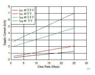
| TA = 25°C | CL = 15 pF |
(With 15-pF Load)
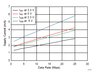
| TA = 25°C | CL = 15 pF |
(With 15-pF Load)
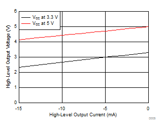
| TA = 25°C |

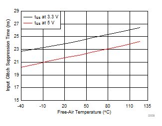

| TA = 25°C | CL = No Load |
(With No Load)
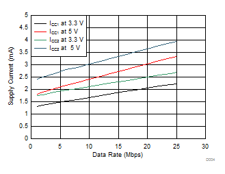
| TA = 25°C | CL = No Load |
(With No Load)

| TA = 25°C |
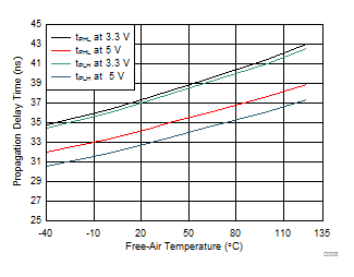

| TA = 25°C |
7 Parameter Measurement Information


tr ≤ 3 ns, tf ≤ 3 ns, ZO = 50 Ω.


8 Detailed Description
8.1 Overview
The isolator in Figure 15 is based on a capacitive isolation barrier technique. The I/O channel of the device consists of two internal data channels, a high-frequency (HF) channel with a bandwidth from 100 kbps up to 25 Mbps, and a low-frequency (LF) channel covering the range from 100 kbps down to DC.
In principle, a single-ended input signal entering the HF channel is split into a differential signal via the inverter gate at the input. The following capacitor-resistor networks differentiate the signal into transient pulses, which then are converted into CMOS levels by a comparator. The transient pulses at the input of the comparator can be either above or below the common mode voltage VREF depending on whether the input bit transitioned from 0 to 1 or 1 to 0. The comparator threshold is adjusted based on the expected bit transition. A decision logic (DCL) at the output of the HF channel comparator measures the durations between signal transients. If the duration between two consecutive transients exceeds a certain time limit, (as in the case of a low-frequency signal), the DCL forces the output-multiplexer to switch from the high-frequency to the low-frequency channel.
8.2 Functional Block Diagram

Because low-frequency input signals require the internal capacitors to assume prohibitively large values, these signals are pulse-width modulated (PWM) with the carrier frequency of an internal oscillator, thus creating a sufficiently high frequency, capable of passing the capacitive barrier. As the input is modulated, a low-pass filter (LPF) is needed to remove the high-frequency carrier from the actual data before passing it on to the output multiplexer.
8.3 Feature Description
| ORDERABLE DEVICE | CHANNEL DIRECTION | RATED ISOLATION | MAX DATA RATE | DEFAULT OUTPUT |
|---|---|---|---|---|
| ISO7330CQDWQ1 and ISO7330CQDWRQ1 | 3 Forward, 0 Reverse |
3000 VRMS / 4242 VPK (1) | 25 Mbps | High |
| ISO7330FCQDWQ1 and ISO7330FCQDWRQ1 | Low | |||
| ISO7331CQDWQ1 and ISO7331CQDWRQ1 | 2 Forward, 1 Reverse |
High | ||
| ISO7331FCQDWQ1 and ISO7331FCQDWRQ1 | Low |
8.3.1 High Voltage Feature Description
8.3.1.1 Package Insulation Specifications
over recommended operating conditions (unless otherwise noted)| PARAMETER | TEST CONDITIONS | MIN | TYP | MAX | UNIT | ||
|---|---|---|---|---|---|---|---|
| L(I01) | Minimum air gap (clearance) | Shortest terminal-to-terminal distance through air | 8 | mm | |||
| L(I02) | Minimum external tracking (creepage) | Shortest terminal-to-terminal distance across the package surface | 8 | mm | |||
| CTI | Tracking resistance (comparative tracking index) | DIN EN 60112 (VDE 0303-11); IEC 60112 | >400 | V | |||
| DTI | Minimum internal gap (internal clearance) | Distance through the insulation | 13 | µm | |||
| RIO | Isolation resistance, input to output(1) | VIO = 500 V, TA = 25°C | >1012 | Ω | |||
| VIO = 500 V, 100°C ≤ TA ≤ max | >1011 | Ω | |||||
| CIO | Isolation capacitance, input to output(1) | VIO = 0.4 sin (2πft), f = 1 MHz | 2 | pF | |||
| CI | Input capacitance(2) | VI = VCC/2 + 0.4 sin (2πft), f = 1 MHz, VCC = 5 V | 2 | pF | |||
NOTE
Creepage and clearance requirements should be applied according to the specific equipment isolation standards of an application. Care should be taken to maintain the creepage and clearance distance of a board design to ensure that the mounting pads of the isolator on the printed-circuit board do not reduce this distance.
Creepage and clearance on a printed-circuit board become equal in certain cases. Techniques such as inserting grooves and/or ribs on a printed circuit board are used to help increase these specifications.
8.3.1.2 Insulation Characteristics
over recommended operating conditions (unless otherwise noted)| PARAMETER(1) | TEST CONDITIONS | SPECIFICATION | UNIT | |
|---|---|---|---|---|
| VIOWM | Maximum isolation working voltage | 1000 | VRMS | |
| VIORM | Maximum repetitive peak voltage per DIN V VDE V 0884-10 |
1414 | VPK | |
| VPR | Input-to-output test voltage per DIN V VDE V 0884-10 |
After Input/Output safety test subgroup 2/3, VPR = VIORM × 1.2, t = 10 s, Partial discharge < 5 pC |
1697 | VPK |
| Method a, After environmental tests subgroup 1, VPR = VIORM × 1.6, t = 10 s, Partial Discharge < 5 pC |
2262 | |||
| Method b1, VPR = VIORM × 1.875, t = 1 s (100% Production test) Partial discharge < 5 pC |
2651 | |||
| VIOTM | Maximum transient overvoltage per DIN V VDE V 0884-10 |
VTEST = VIOTM
t = 60 sec (qualification) t= 1 sec (100% production) |
4242 | VPK |
| VIOSM | Maximum surge isolation voltage per DIN V VDE V 0884-10 |
Test method per IEC 60065, 1.2/50 µs waveform, VTEST = 1.3 × VIOSM = 7800 VPK (qualification) |
6000 | VPK |
| VISO | Withstand isolation voltage per UL 1577 | VTEST = VISO = 3000 VRMS, t = 60 sec (qualification) VTEST = 1.2 × VISO = 3600 VRMS, t = 1 sec (100% production) |
3000 | VRMS |
| RS | Insulation resistance | VIO = 500 V at TS | >109 | Ω |
| Pollution degree | 2 | |||
Table 1. IEC 60664-1 Ratings Table
| PARAMETER | TEST CONDITIONS | SPECIFICATION |
|---|---|---|
| Basic isolation group | Material group | II |
| Installation classification | Rated mains voltage ≤ 300 VRMS | I–IV |
| Rated mains voltage ≤ 600 VRMS | I–III | |
| Rated mains voltage ≤ 1000 VRMS | I–II |
8.3.1.3 Regulatory Information
| VDE | CSA | UL | CQC |
|---|---|---|---|
| Certified according to DIN V VDE V 0884-10 (VDE V 0884-10):2006-12 and DIN EN 61010-1 (VDE 0411-1):2011-07 | Approved under CSA Component Acceptance Notice 5A, IEC 60950-1, and IEC 61010-1 | Recognized under UL 1577 Component Recognition Program | Planned to be certified according to GB4943.1-2011 |
| Basic Insulation Maximum Transient Overvoltage, 4242 VPK ; Maximum Surge Isolation Voltage, 6000 VPK; Maximum Repetitive Peak Isolation Voltage', 1414 VPK |
800 VRMS Basic Insulation and 400 VRMS Reinforced Insulation working voltage per CSA 60950-1-07+A1+A2 and IEC 60950-1 2nd Ed.+A1+A2; 300 VRMS Basic Insulation working voltage per CSA 61010-1-12 and IEC 61010-1 3rd Ed. |
Single protection, 3000 VRMS (1) | Reinforced Insulation, Altitude ≤ 5000 m, Tropical Climate, 250 VRMS maximum working voltage |
| Certificate number: 40016131 | Master contract number: 220991 | File number: E181974 | Certification planned |
8.3.1.4 Safety Limiting Values
Safety limiting intends to minimize potential damage to the isolation barrier upon failure of input or output circuitry. A failure of the I/O can allow low resistance to ground or the supply and, without current limiting, dissipate sufficient power to overheat the die and damage the isolation barrier, potentially leading to secondary system failures.| PARAMETER | TEST CONDITIONS | MIN | TYP | MAX | UNIT | |
|---|---|---|---|---|---|---|
| IS | Safety input, output, or supply current | RθJA = 78.3 °C/W, VI = 5.5 V, TJ = 150°C, TA = 25°C | 290 | mA | ||
| RθJA = 78.3 °C/W, VI = 3.6 V, TJ = 150°C, TA = 25°C | 443 | |||||
| TS | Maximum safety temperature | 150 | °C | |||
The safety-limiting constraint is the absolute-maximum junction temperature specified in the Absolute Maximum Ratings table. The power dissipation and junction-to-air thermal impedance of the device installed in the application hardware determines the junction temperature. The assumed junction-to-air thermal resistance in the Thermal Information table is that of a device installed on a High-K Test Board for Leaded Surface-Mount Packages. The power is the recommended maximum input voltage times the current. The junction temperature is then the ambient temperature plus the power times the junction-to-air thermal resistance.
 Figure 16. Thermal Derating Curve per VDE
8.4 Device Functional Modes
Table 2 lists the functional modes for the ISO733x-Q1 family of devices.
Table 2. Function Table(1)
| VCCI | VCCO | INPUT (INx) |
OUTPUT ENABLE (ENx) |
OUTPUT (OUTx) |
|
|---|---|---|---|---|---|
| ISO733xCQDWQ1 AND ISO733xCQDWRQ1 | ISO733xFCQDWQ1 AND ISO733xFCQDWRQ1 | ||||
| PU | PU | H | H or Open | H | H |
| L | H or Open | L | L | ||
| X | L | Z | Z | ||
| Open | H or Open | H(2) | L(3) | ||
| PD | PU | X | H or Open | H(2) | L(3) |
| X | PU | X | L | Z | Z |
| X | PD | X | X | Undetermined | Undetermined |
8.4.1 Device I/O Schematics
 Figure 17. Device I/O Schematics
9 Application and Implementation
NOTE
Information in the following applications sections is not part of the TI component specification, and TI does not warrant its accuracy or completeness. TI’s customers are responsible for determining suitability of components for their purposes. Customers should validate and test their design implementation to confirm system functionality.
9.1 Application Information
The ISO733x-Q1 family of devices uses single-ended TTL-logic switching technology. Its supply voltage range is from 3 V to 5.5 V for both supplies, VCC1 and VCC2. When designing with digital isolators, keep in mind that because of the single-ended design structure, digital isolators do not conform to any specific interface standard and are only intended for isolating single-ended CMOS or TTL digital signal lines. The isolator is typically placed between the data controller (that is, μC or UART), and a data converter or a line transceiver, regardless of the interface type or standard.
9.2 Typical Application
The ISO7331-Q1 device combined with Texas Instruments' Piccolo™ microcontroller, analog-to-digital receiver, transformer driver, and voltage regulator can create an isolated serial peripheral interface (SPI) as shown in Figure 18.

9.2.1 Design Requirements
9.2.1.1 Typical Supply Current Equations
For the equations in this section, the following is true:
- ICC1 and ICC2 are typical supply currents measured in mA
- f is the data rate measured in Mbps
- CL is the capacitive load measured in pF
9.2.1.1.1 ISO7330-Q1
At VCC1 = VCC2 = 5 V
At VCC1 = VCC2 = 3.3 V
9.2.1.1.2 ISO7321-Q1
At VCC1 = VCC2 = 5 V
At VCC1 = VCC2 = 3.3 V
9.2.2 Detailed Design Procedure
9.2.2.1 Electromagnetic Compatibility (EMC) Considerations
Many applications in harsh industrial environment are sensitive to disturbances such as electrostatic discharge (ESD), electrical fast transient (EFT), surge and electromagnetic emissions. These electromagnetic disturbances are regulated by international standards such as IEC 61000-4-x and CISPR 22. Although system-level performance and reliability depends, to a large extent, on the application board design and layout, the ISO733x-Q1 family of devices incorporates many chip-level design improvements for overall system robustness. Some of these improvements include:
- Robust ESD protection cells for input and output signal pins and inter-chip bond pads.
- Low-resistance connectivity of ESD cells to supply and ground pins.
- Enhanced performance of high voltage isolation capacitor for better tolerance of ESD, EFT and surge events.
- Bigger on-chip decoupling capacitors to bypass undesirable high energy signals through a low impedance path.
- PMOS and NMOS devices isolated from each other by using guard rings to avoid triggering of parasitic SCRs.
- Reduced common mode currents across the isolation barrier by ensuring purely differential internal operation.
9.2.3 Application Curves
The following typical eye diagrams of the ISO733x-Q1 family of devices indicate low jitter and wide open eye at the maximum data rate of 25 Mbps.
 Figure 19. Eye Diagram at 25 Mbps, 5 V and 25°C
 Figure 20. Eye Diagram at 25 Mbps, 3.3 V and 25°C
9.2.4 Systems Examples
Unlike optocouplers, which require external components to improve performance, provide bias, or limit current, the ISO733x-Q1 family of devices only requires two external bypass capacitors to operate.
 Figure 21. Typical ISO7330-Q1 Circuit Hook-up
 Figure 22. Typical ISO7331-Q1 Circuit Hook-up