-
ISO7420FCC Low-Power Dual Channel Digital Isolator
- 1 Features
- 2 Applications
- 3 Description
- 4 Revision History
- 5 Pin Configuration and Functions
-
6 Specifications
- 6.1 Absolute Maximum Ratings
- 6.2 ESD Ratings
- 6.3 Recommended Operating Conditions
- 6.4 Thermal Information
- 6.5 Electrical Characteristics: VCC1 and VCC2 = 5 V ± 10%
- 6.6 Electrical Characteristics: VCC1 and VCC2 = 3.3 V ± 10%
- 6.7 Electrical Characteristics: VCC1 and VCC2 = 2.7 V
- 6.8 Power Dissipation Characteristics
- 6.9 Switching Characteristics: VCC1 and VCC2 = 5 V ± 10%
- 6.10 Switching Characteristics: VCC1 and VCC2 = 3.3 V ± 10%
- 6.11 Switching Characteristics: VCC1 and VCC2 = 2.7 V
- 6.12 Typical Characteristics
- 7 Parameter Measurement Information
- 8 Detailed Description
- 9 Application and Implementation
- 10Power Supply Recommendations
- 11Layout
- 12Device and Documentation Support
- 13Mechanical, Packaging, and Orderable Information
- IMPORTANT NOTICE
Package Options
Mechanical Data (Package|Pins)
- D|8
Thermal pad, mechanical data (Package|Pins)
Orderable Information
ISO7420FCC Low-Power Dual Channel Digital Isolator
1 Features
- Signaling Rate: 50 Mbps (5-V Supplies)
- Output is Low in Default Mode
- Integrated Noise Filter on the Input Pins
- Low Power Consumption: Typical ICC per Channel
- 1.8 mA at 1 Mbps, 3.9 mA at 25 Mbps (5-V Supplies)
- 1.4 mA at 1 Mbps, 2.6 mA at 25 Mbps (3.3-V Supplies)
- Low Propagation Delay: 20 ns Typical (5-V Supplies)
- Channel-to-Channel Output Skew: 2 ns Maximum
- 3.3-V and 5-V Level Translation
- Wide TA Range Specified: –40°C to 125°C
- 60-KV/μs Transient Immunity, Typical (5-V Supplies)
- Low Emissions
- Isolation Barrier Life: > 25 Years
- Operates from 2.7-V to 5.5-V Supply Levels
- Narrow Body SOIC-8 Package
- Safety and Regulatory Approvals
2 Applications
- Opto-Coupler Replacement in:
- Industrial FieldBus
- ProfiBus
- ModBus
- DeviceNet™ Data Buses
- Servo Control Interface
- Motor Control
- Power Supplies
- Battery Packs
- Industrial FieldBus
3 Description
ISO7420FCC provides galvanic isolation up to 2500 VRMS for 1 minute per UL and 4242 VPK per VDE. This device has two isolated channels. Each channel has a logic input and output buffer separated by a silicon dioxide (SiO2) insulation barrier. Used in conjunction with isolated power supplies, this device prevents noise currents on a data bus or other circuit from entering the local ground and interfering with or damaging sensitive circuitry. The suffix F indicates low-output option in fail-safe conditions (see Table 2). This device has integrated noise filter for harsh environments where short noise pulses may be present at the device input pins.
ISO7420FCC has TTL input thresholds and operates from 2.7-V to 5.5-V supplies. All inputs are 5-V tolerant when supplied from a 2.7-V or 3.3-V supply.
Device Information(1)
| PART NUMBER | PACKAGE | BODY SIZE (NOM) |
|---|---|---|
| ISO7420FCC | SOIC (8) | 4.90 mm × 3.91 mm |
- For all available packages, see the orderable addendum at the end of the datasheet.
Simplified Schematic

4 Revision History
Changes from B Revision (January 2014) to C Revision
- Added Pin Configuration and Functions section, ESD Ratings table, Feature Description section, Device Functional Modes, Application and Implementation section, Power Supply Recommendations section, Layout section, Device and Documentation Support section, and Mechanical, Packaging, and Orderable Information section Go
- VDE standard changed to DIN V VDE V 0884-10 (VDE V 0884-10): 2006-12 Go
- Changed VDE standard changed to DIN V VDE V 0884-10 (VDE V 0884-10):2006-12 Go
- Changed Note 1 Figure 12Go
- Changed Figure 13Go
Changes from A Revision (July 2013) to B Revision
- Changed the SAFETY AND REGULATORY APPROVALS listGo
- Changed the VIH MAX value From: VCC To: 5.5V in the RECOMMENDED OPERATING CONDITIONS table Go
- Changed the VPR and VIOTM parameter From: DIN EN 60747-5-2 To: DIN EN 60747-5-5 in the INSULATION CHARACTERISTICS tableGo
- Changed the REGULATORY INFORMATION tableGo
- Changed the title of Figure 16 From: θJC Thermal Derating Curve per DIN EN 60747-5-2 To: θJC Thermal Derating Curve per DIN EN 60747-5-5Go
Changes from * Revision (June 2013) to A Revision
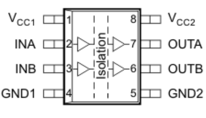
5 Pin Configuration and Functions

Pin Functions
| PIN | I/O | DESCRIPTION | |
|---|---|---|---|
| NAME | NO. | ||
| GND1 | 4 | – | Ground connection for VCC1 |
| GND2 | 5 | – | Ground connection for VCC2 |
| INA | 2 | I | Input, channel A |
| INB | 3 | I | Input, channel B |
| OUTA | 7 | O | Output, channel A |
| OUTB | 6 | O | Output, channel B |
| VCC1 | 1 | – | Power supply, VCC1 |
| VCC2 | 8 | – | Power supply, VCC2 |