JAJSAD1G April 2005 – May 2016 ADC081S021
PRODUCTION DATA.
- 1 特長
- 2 アプリケーション
- 3 概要
- 4 改訂履歴
- 5 Device Comparison Table
- 6 Pin Configuration and Functions
- 7 Specifications
- 8 Detailed Description
- 9 Application and Implementation
- 10Power Supply Recommendations
- 11Layout
- 12デバイスおよびドキュメントのサポート
- 13メカニカル、パッケージ、および注文情報
パッケージ・オプション
メカニカル・データ(パッケージ|ピン)
サーマルパッド・メカニカル・データ
発注情報
11 Layout
11.1 Layout Guidelines
Capacitive coupling between noisy digital circuitry and sensitive analog circuitry can lead to poor performance. TI strongly recommends keeping the analog and digital circuitry separated from each other and the clock line as short as possible.
Digital circuits create substantial supply and ground current transients. This digital noise could have significant impact upon system noise performance. To avoid performance degradation due to supply noise, do not use the same supply for the ADC081S021 that is used for digital logic.
Generally, analog and digital lines must cross each other at 90° to avoid crosstalk. However, to maximize accuracy in high resolution systems, avoid crossing analog and digital lines altogether. It is important to keep clock lines as short as possible and isolated from ALL other lines, including other digital lines. In addition, the clock line must also be treated as a transmission line and be properly terminated.
The analog input must be isolated from noisy signal lines to avoid coupling of spurious signals into the input. Any external component (that is, a filter capacitor) connected between the converter’s input pins and ground or to the reference input pin and ground must be connected to a very clean point in the ground plane.
TI recommends the use of a single, uniform ground plane and the use of split power planes. The power planes must be placed within the same board layer. All analog circuitry (input amplifiers, filters, reference components, and so on) must be placed over the analog power plane. All digital circuitry and I/O lines must be placed over the digital power plane. In addition, all components in the reference circuitry and the input signal chain that are connected to ground must be connected together with short traces and enter the analog ground plane at a single, quiet point.
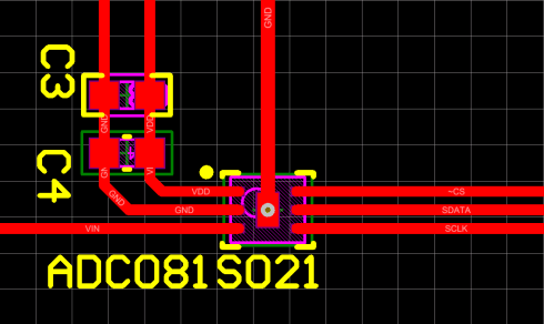
11.2 Layout Example
 Figure 27. DBV Package Layout
 Figure 28. NGF Package Layout