SNAS304H January 2006 – April 2016 ADC121S101 , ADC121S101-Q1
PRODUCTION DATA.
- 1 Features
- 2 Applications
- 3 Description
- 4 Revision History
- 5 Device Comparison Table
- 6 Pin Configuration and Functions
- 7 Specifications
- 8 Detailed Description
- 9 Application and Implementation
- 10Power Supply Recommendations
- 11Layout
- 12Device and Documentation Support
- 13Mechanical, Packaging, and Orderable Information
9 Application and Implementation
NOTE
Information in the following applications sections is not part of the TI component specification, and TI does not warrant its accuracy or completeness. TI’s customers are responsible for determining suitability of components for their purposes. Customers should validate and test their design implementation to confirm system functionality.
9.1 Application Information
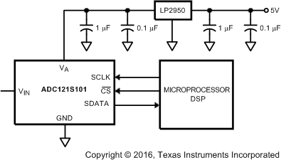
Figure 22 shows a typical application of the ADC. In this example, power is provided by TI's LP2950 low-dropout voltage regulator, available in a variety of fixed and adjustable output voltages. The power supply pin is bypassed with a capacitor network placed close to the ADC. Because the reference for the ADC is the supply voltage, any noise on the supply degrades the noise performance of the device. To keep noise off the supply, use a dedicated linear regulator for this device, or provide sufficient decoupling from other circuitry to keep noise off the ADC supply pin. Because of the ADC's low power requirements, it is also possible to use a precision reference as a power supply to maximize performance. The three-wire interface is shown in Figure 22 connected to a microprocessor or DSP.
9.2 Typical Application
 Figure 22. Typical Application Circuit
9.2.1 Design Requirements
A positive supply-only, data acquisition system is capable of digitizing a single-ended input signal ranging from
0 V to 5 V with a throughput up to 1 Msps. The ADC121S101 must interface to an MCU whose supply is set at
5 V.
9.2.2 Detailed Design Procedure
The signal range requirement forces the design to use 5-V analog supply at VA, analog supply. This follows from the fact that VA is also a reference potential for the ADC. The maximum sampling rate of the ADC121S101
Fs = FSCLK / 20.
Noise consideration must be given to the SPI interface, especially when the master MCU is capable of producing fast rising edges on the digital bus signals. Inserting small resistances in the digital signal path may help in reducing the ground bounce, and thus improve the overall noise performance of the system.
Take care when the signal source is capable of producing voltages beyond VA. In such instances, the internal ESD diodes may start conducting. The ESD diodes are not intended as input signal clamps. To provide the desired clamping action use Schottky diodes.
A 0.1-µF capacitor must be placed close to the supply pin of the ADC121S101.
A small capacitor (1 nF to 10 nF) placed on the input pin can help the internal sampling capacitor settle. If the ADC121S101 is driven by an operational amplifier, a small resistor (50 Ω to 200 Ω) must be placed between the output of the operational amplifier and the junction of the capacitor and the ADC121S101 input pin.
9.2.3 Application Curve
 Figure 23. ADC Transfer Characteristic