-
ADC121S101x Single-Channel, 0.5 to 1-Msps, 12-Bit Analog-to-Digital Converter SNAS304H January 2006 – April 2016 ADC121S101 , ADC121S101-Q1
PRODUCTION DATA.
-
ADC121S101x Single-Channel, 0.5 to 1-Msps, 12-Bit Analog-to-Digital Converter
- 1 Features
- 2 Applications
- 3 Description
- 4 Revision History
- 5 Device Comparison Table
- 6 Pin Configuration and Functions
- 7 Specifications
- 8 Detailed Description
- 9 Application and Implementation
- 10Power Supply Recommendations
- 11Layout
- 12Device and Documentation Support
- 13Mechanical, Packaging, and Orderable Information
- IMPORTANT NOTICE
ADC121S101x Single-Channel, 0.5 to 1-Msps, 12-Bit Analog-to-Digital Converter
1 Features
2 Applications
- Portable Systems
- Remote Data Acquisition
- Instrumentation and Control Systems
- Automotive
3 Description
The ADC121S101 is a low-power, single-channel CMOS 12-bit analog-to-digital converter with a high-speed serial interface. Unlike the conventional practice of specifying performance at a single sample rate only, the ADC121S101 is fully specified over a sample rate range of 500 ksps to 1 Msps. The converter is based upon a successive-approximation register architecture with an internal track-and-hold circuit.
The output serial data is straight binary, and is compatible with several standards, such as SPI™, QSPI™, MICROWIRE, and many common DSP serial interfaces.
The ADC121S101 operates with a single supply with a range from 2.7 V to 5.25 V. Normal power consumption using a 3 V or 5 V supply is 2 mW and 10 mW, respectively. The power-down feature reduces the power consumption to as low as 2.6 µW using a 5-V supply.
The ADC121S101 is packaged in 6-pin WSON and SOT-23 packages. Operation over the temperature range of −40°C to 125°C is specified.
Device Information(1)
| PART NUMBER | PACKAGE | BODY SIZE (NOM) |
|---|---|---|
| ADC121S101 | WSON (6) | 2.50 mm × 2.20 mm |
| SOT-23 (6) | 2.90 mm × 1.60 mm |
- For all available packages, see the orderable addendum at the end of the data sheet.
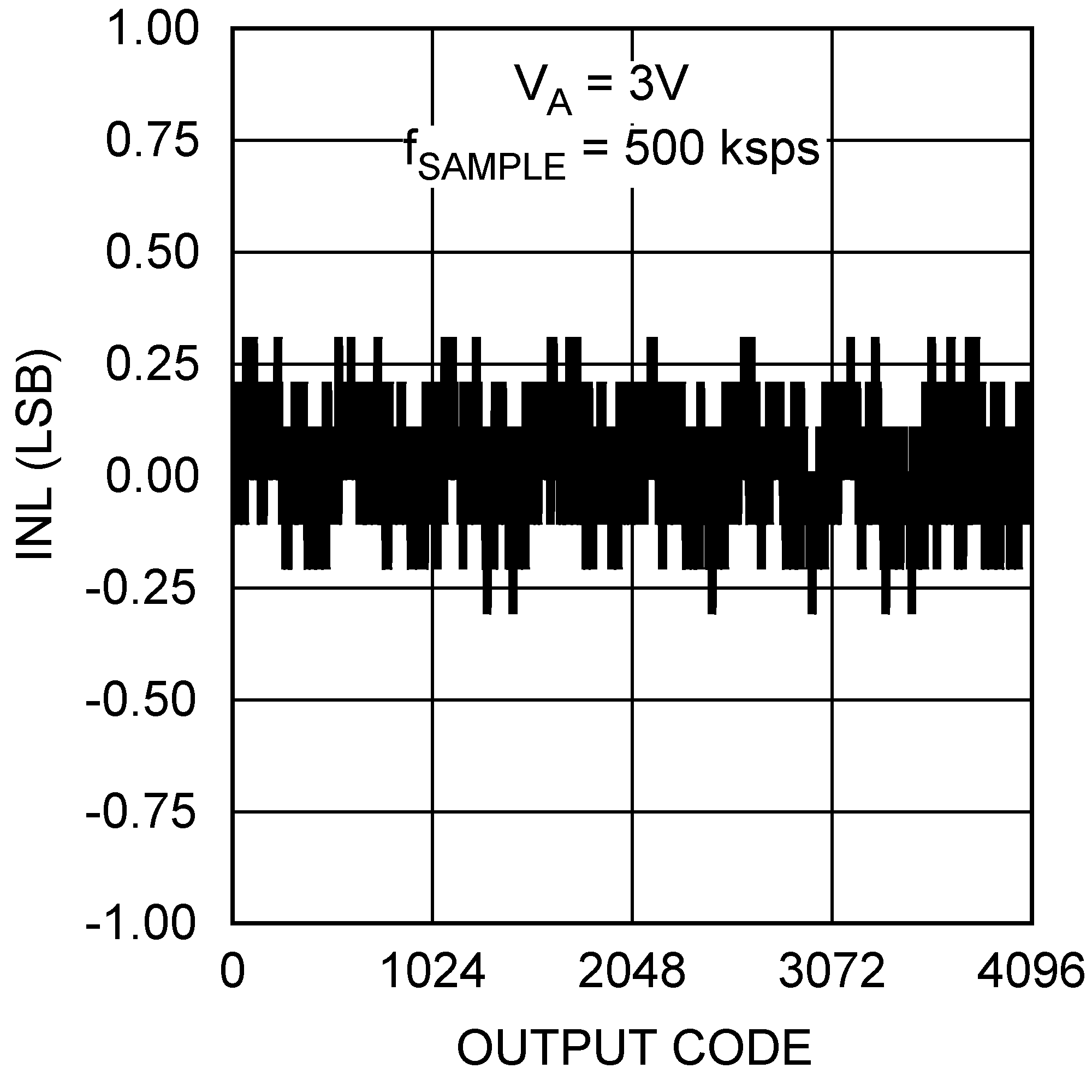
INL, fSCLK = 10 MHz
4 Revision History
Changes from G Revision (January 2014) to H Revision
- Added ESD Ratings table, Feature Description section, Device Functional Modes, Application and Implementation section, Power Supply Recommendations section, Layout section, Device and Documentation Support section, and Mechanical, Packaging, and Orderable Information sectionGo
Changes from F Revision (May 2013) to G Revision
- Changed sentence in the Using the ADC121S101 sectionGo
Changes from E Revision (May 2013) to F Revision
- Changed layout of National Data Sheet to TI formatGo
5 Device Comparison Table(1)
| RESOLUTION | SPECIFIED SAMPLE RATE RANGE | ||
|---|---|---|---|
| 50 TO 200 KSPS | 200 TO 500 KSPS | 500 KSPS TO 1 MSPS | |
| 12 Bits | ADC121S021 | ADC121S051 | ADC121S101 |
| 10 Bits | ADC101S021 | ADC101S051 | ADC101S101 |
| 8 Bits | ADC081S021 | ADC081S051 | ADC081S101 |
6 Pin Configuration and Functions
Pin Functions
| PIN | TYPE(1) | DESCRIPTION | |
|---|---|---|---|
| NO. | NAME | ||
| 1 | VA | P | Positive supply pin. This pin must be connected to a quiet 2.7-V to 5.25-V source and bypassed to GND with a 1-µF capacitor and a 0.1-µF monolithic capacitor located within 1 cm of the power pin. |
| 2 | GND | G | The ground return for the supply and signals. |
| 3 | VIN | I | Analog input. This signal can range from 0 V to VA. |
| 4 | SCLK | I | Digital clock input. This clock directly controls the conversion and readout processes. |
| 5 | SDATA | O | Digital data output. The output samples are clocked out of this pin on falling edges of the SCLK pin. |
| 6 | CS | I | Chip select. On the falling edge of CS, a conversion process begins. |
| PAD | GND | G | For package suffix CISD(X) only. TI recommends connecting the center pad to ground. |
7 Specifications
7.1 Absolute Maximum Ratings
over operating free-air temperature range (unless otherwise noted)(1)(2)(3)| MIN | MAX | UNIT | ||
|---|---|---|---|---|
| Analog supply voltage, VA | –0.3 | 6.5 | V | |
| Voltage on any digital pin to GND | –0.3 | 6.5 | V | |
| Voltage on any analog pin to GND | –0.3 | VA + 0.3 | V | |
| Input current at any pin(4) | ±10 | mA | ||
| Package input current(4) | ±20 | mA | ||
| Power consumption at TA = 25°C | See(5) | |||
| Junction temperature, TJ | 150 | °C | ||
| Storage temperature, Tstg | –65 | 150 | °C | |
7.2 ESD Ratings: ADC121S101
| VALUE | UNIT | |||
|---|---|---|---|---|
| V(ESD) | Electrostatic discharge | Human-body model (HBM), per ANSI/ESDA/JEDEC JS-001(1) | ±3500 | V |
| Machine model (MM) | ±300 | |||
7.3 ESD Ratings: ADC121S101-Q1
| VALUE | UNIT | ||||
|---|---|---|---|---|---|
| V(ESD) | Electrostatic discharge | Human-body model (HBM), per AEC Q100-002(1) | ±3500 | V | |
| Charged-device model (CDM), per AEC Q100-011, all pins | ±300 | ||||
7.4 Recommended Operating Conditions
over operating free-air temperature range (unless otherwise noted)(1)| MIN | NOM | MAX | UNIT | ||
|---|---|---|---|---|---|
| VA | Supply voltage | 2.7 | 5.25 | V | |
| Digital input pins voltage (regardless of supply voltage) | –0.3 | 5.25 | V | ||
| Analog input pins voltage | 0 | VA | V | ||
| Clock frequency | 25 | 20000 | kHz | ||
| Sample rate | Up to 1 Msps |
||||
| TA | Operating temperature | –40 | 125 | °C | |
7.5 Thermal Information
| THERMAL METRIC(1) | ADC121S101 | UNIT | ||
|---|---|---|---|---|
| NGF (WSON) | DBV (SOT-23) | |||
| 6 PINS | 6 PINS | |||
| RθJA | Junction-to-ambient thermal resistance | 94 | 265 | °C/W |
| RθJC(top) | Junction-to-case (top) thermal resistance | 118 | 151 | °C/W |
| RθJB | Junction-to-board thermal resistance | 69 | 30 | °C/W |
| ψJT | Junction-to-top characterization parameter | 6.5 | 30 | °C/W |
| ψJB | Junction-to-board characterization parameter | 69 | 29 | °C/W |
| RθJC(bot) | Junction-to-case (bottom) thermal resistance | 15 | N/A | °C/W |
7.6 Electrical Characteristics
VA = 2.7 V to 5.25 V, GND = 0 V, fSCLK = 10 MHz to 20 MHz, CL = 15 pF, fSAMPLE = 500 ksps to 1 Msps, and TA = 25°C (unless otherwise noted)(1)| PARAMETER | TEST CONDITIONS | MIN(2) | TYP | MAX(2) | UNIT | ||
|---|---|---|---|---|---|---|---|
| STATIC CONVERTER | |||||||
| Resolution with no missing codes | VA = 2.7 V to 3.6 V, –40°C ≤ TA ≤ 125°C | 12 | Bits | ||||
| INL | Integral non-linearity | –40°C ≤ TA ≤ 85°C, VA = 2.7 V to 3.6 V |
SOT-23 | –1 | ±0.4 | 1 | LSB |
| WSON | –1.2 | ±0.4 | 1 | ||||
| TA = 125°C, VA = 2.7 V to 3.6 V |
SOT-23 | –1.1 | 1 | ||||
| WSON | –1.3 | 1 | |||||
| DNL | Differential non-linearity | –40°C ≤ TA ≤ 85°C, VA = 2.7 V to 3.6 V | 0.5 | 1 | LSB | ||
| –0.9 | –0.3 | ||||||
| TA = 125°C, VA = 2.7 V to 3.6 V | –1 | 1 | |||||
| VOFF | Offset error | –40°C ≤ TA ≤ 125°C, VA = 2.7 V to 3.6 V | –1.2 | ±0.1 | 1.2 | LSB | |
| GE | Gain error | –40°C ≤ TA ≤ 125°C, VA = 2.7 V to 3.6 V |
SOT-23 | –1.2 | ±0.2 | 1.2 | LSB |
| WSON | –1.5 | ±0.2 | 1.5 | ||||
| DYNAMIC CONVERTER | |||||||
| SINAD | Signal-to-noise plus distortion ratio | VA = 2.7 V to 5.25 V, –40°C ≤ TA ≤ 125°C fIN = 100 kHz, –0.02 dBFS |
70 | 72 | dB | ||
| SNR | Signal-to-noise ratio | VA = 2.7 V to 5.25 V, –40°C ≤ TA ≤ 85°C fIN = 100 kHz, –0.02 dBFS |
70.8 | 72.5 | dB | ||
| VA = 2.7 V to 5.25 V, TA = 125°C fIN = 100 kHz, –0.02 dBFS |
70.6 | ||||||
| THD | Total harmonic distortion | VA = 2.7 V to 5.25 V, fIN = 100 kHz, –0.02 dBFS |
–80 | dB | |||
| SFDR | Spurious-free dynamic range | VA = 2.7 V to 5.25 V, fIN = 100 kHz, –0.02 dBFS |
82 | dB | |||
| ENOB | Effective number of bits | VA = 2.7 V to 5.25 V, fIN = 100 kHz, –0.02 dBFS, –40°C ≤ TA ≤ 125°C |
11.3 | 11.6 | Bits | ||
| IMD | Intermodulation distortion, second order terms |
VA = 5.25 V, fa = 103.5 kHz, fb = 113.5 kHz | –78 | dB | |||
| Intermodulation distortion, third order terms |
VA = 5.25 V, fa = 103.5 kHz, fb = 113.5 kHz | –78 | dB | ||||
| FPBW | –3-dB full power bandwidth | VA = 5 V | 11 | MHz | |||
| VA = 3 V | 8 | ||||||
| ANALOG INPUT | |||||||
| VIN | Input range | 0 to VA | V | ||||
| IDCL | DC leakage current | –40°C ≤ TA ≤ 125°C | –1 | 1 | µA | ||
| CINA | Input capacitance | Track mode | 30 | pF | |||
| Hold mode | 4 | ||||||
| DIGITAL INPUT | |||||||
| VIH | Input high voltage | VA = 5.25 V, –40°C ≤ TA ≤ 125°C | 2.4 | V | |||
| VA = 3.6 V, –40°C ≤ TA ≤ 125°C | 2.1 | ||||||
| VIL | Input low voltage | VA = 5 V, –40°C ≤ TA ≤ 125°C | 0.8 | V | |||
| VA = 3 V, –40°C ≤ TA ≤ 125°C | 0.4 | ||||||
| IIN | Input current | VIN = 0 V or VA, –40°C ≤ TA ≤ 125°C | –1 | ±0.1 | 1 | µA | |
| CIND | Digital input capacitance | –40°C ≤ TA ≤ 125°C | 2 | 4 | pF | ||
| DIGITAL OUTPUT | |||||||
| VOH | Output high voltage | ISOURCE = 200 µA, –40°C ≤ TA ≤ 125°C | VA – 0.2 | VA – 0.07 | V | ||
| ISOURCE = 1 mA | VA – 0.1 | ||||||
| VOL | Output low voltage | ISINK = 200 µA, –40°C ≤ TA ≤ 125°C | 0.03 | 0.4 | V | ||
| ISINK = 1 mA | 0.1 | ||||||
| IOZH, IOZL | TRI-STATE leakage current | –40°C ≤ TA ≤ 125°C | –10 | ±0.1 | 10 | µA | |
| COUT | TRI-STATE output capacitance | –40°C ≤ TA ≤ 125°C | 2 | 4 | pF | ||
| Output coding | Straight (natural) binary | ||||||
| POWER SUPPLY | |||||||
| VA | Supply voltage | –40°C ≤ TA ≤ 125°C | 2.7 | 5.25 | V | ||
| IA | Supply current, normal mode (operational, CS low) |
VA = 5.25 V, fSAMPLE = 1 Msps, –40°C ≤ TA ≤ 125°C |
2.0 | 3.2 | mA | ||
| VA = 3.6 V, fSAMPLE = 1 Msps, –40°C ≤ TA ≤ 125°C |
0.6 | 1.5 | |||||
| Supply current, shutdown (CS high) |
fSCLK = 0 MHz, VA = 5 V, fSAMPLE = 0 ksps | 500 | nA | ||||
| fSCLK = 20 MHz, VA = 5 V, fSAMPLE = 0 ksps | 60 | µA | |||||
| PD | Power consumption, normal mode (operational, CS low) |
VA = 5 V, –40°C ≤ TA ≤ 125°C | 10 | 16 | mW | ||
| VA = 3 V, –40°C ≤ TA ≤ 125°C | 2.0 | 4.5 | |||||
| Power consumption, shutdown (CS high) |
fSCLK = 0 MHz, VA = 5 V, fSAMPLE = 0 ksps | 2.5 | µW | ||||
| fSCLK = 20 MHz, VA = 5 V, fSAMPLE = 0 ksps | 300 | ||||||
| AC | |||||||
| fSCLK | Clock frequency(3) | –40°C ≤ TA ≤ 125°C(4) | 10 | 20 | MHz | ||
| fS | Sample rate | –40°C ≤ TA ≤ 125°C(4) | 500 | 1000 | ksps | ||
| DC | SCLK duty cycle | fSCLK = 20 MHz, –40°C ≤ TA ≤ 125°C | 40% | 50% | 60% | ||
| tACQ | Minimum time required for acquisition | –40°C ≤ TA ≤ 125°C | 350 | ns | |||
| tQUIET | Quiet time | –40°C ≤ TA ≤ 125°C(5) | 50 | ns | |||
| tAD | Aperture delay | 3 | ns | ||||
| tAJ | Aperture jitter | 30 | ps | ||||
7.7 Timing Requirements
VA = 2.7 V to 5.25 V, GND = 0 V, fSCLK = 10 MHz to 20 MHz, CL = 25 pF, fSAMPLE = 500 ksps to 1 Msps, and TA = 25°C (unless otherwise noted)| PARAMETER | TEST CONDITIONS | MIN | TYP | MAX | UNIT | |
|---|---|---|---|---|---|---|
| tCS | Minimum CS pulse width | –40°C ≤ TA ≤ 125°C | 10 | ns | ||
| tSU | CS to SCLK setup time | –40°C ≤ TA ≤ 125°C | 10 | ns | ||
| tEN | Delay from CS until SDATA TRI-STATE disabled(1) | –40°C ≤ TA ≤ 125°C | 20 | ns | ||
| tACC | Data access time after SCLK falling edge(2) | VA = 2.7 V to 3.6 V, –40°C ≤ TA ≤ 125°C |
40 | ns | ||
| VA = 4.75 V to 5.25 V, –40°C ≤ TA ≤ 125°C |
20 | |||||
| tCL | SCLK low pulse width | –40°C ≤ TA ≤ 125°C | 0.4 × tSCLK | ns | ||
| tCH | SCLK high pulse width | –40°C ≤ TA ≤ 125°C | 0.4 × tSCLK | ns | ||
| tH | SCLK to data valid hold time | VA = 2.7 V to 3.6 V, –40°C ≤ TA ≤ 125°C |
7 | ns | ||
| VA = 4.75 V to 5.25 V, –40°C ≤ TA ≤ 125°C |
5 | |||||
| tDIS | SCLK falling edge to SDATA high impedance(3) | VA = 2.7 V to 3.6 V, –40°C ≤ TA ≤ 125°C |
6 | 25 | ns | |
| VA = 4.75 V to 5.25 V, –40°C ≤ TA ≤ 125°C |
5 | 25 | ||||
| tPOWER-UP | Power-up time from full power down | 1 | µs | |||
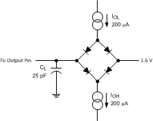 Figure 1. Timing Test Circuit
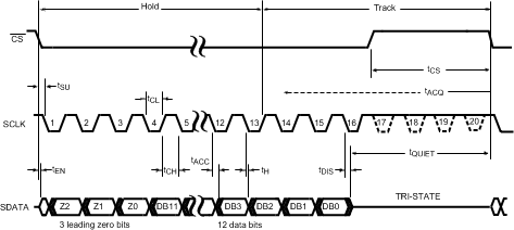 Figure 2. Serial Timing Diagram
7.8 Typical Characteristics
TA = 25°C, fSAMPLE = 500 ksps to 1 Msps, fSCLK = 10 MHz to 20 MHz, and fIN = 100 kHz (unless otherwise noted)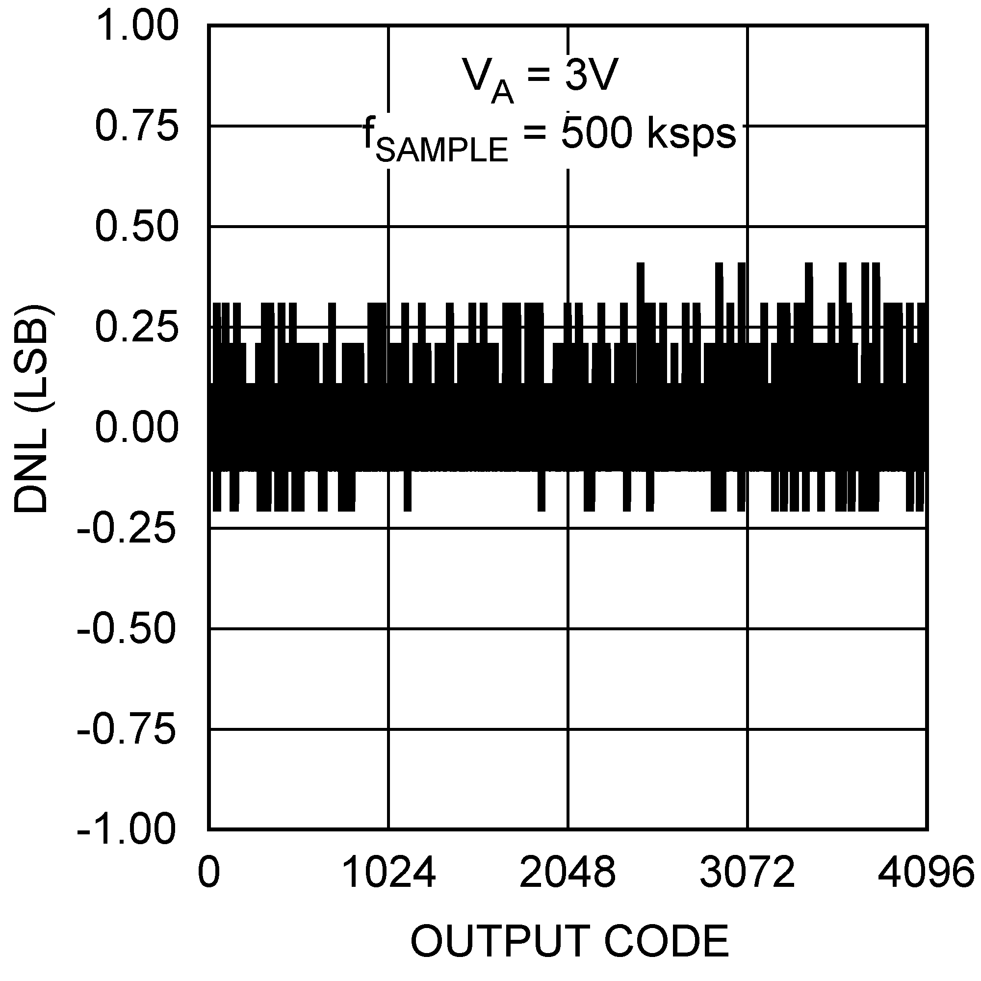 Figure 3. DNL, fSCLK = 10 MHz
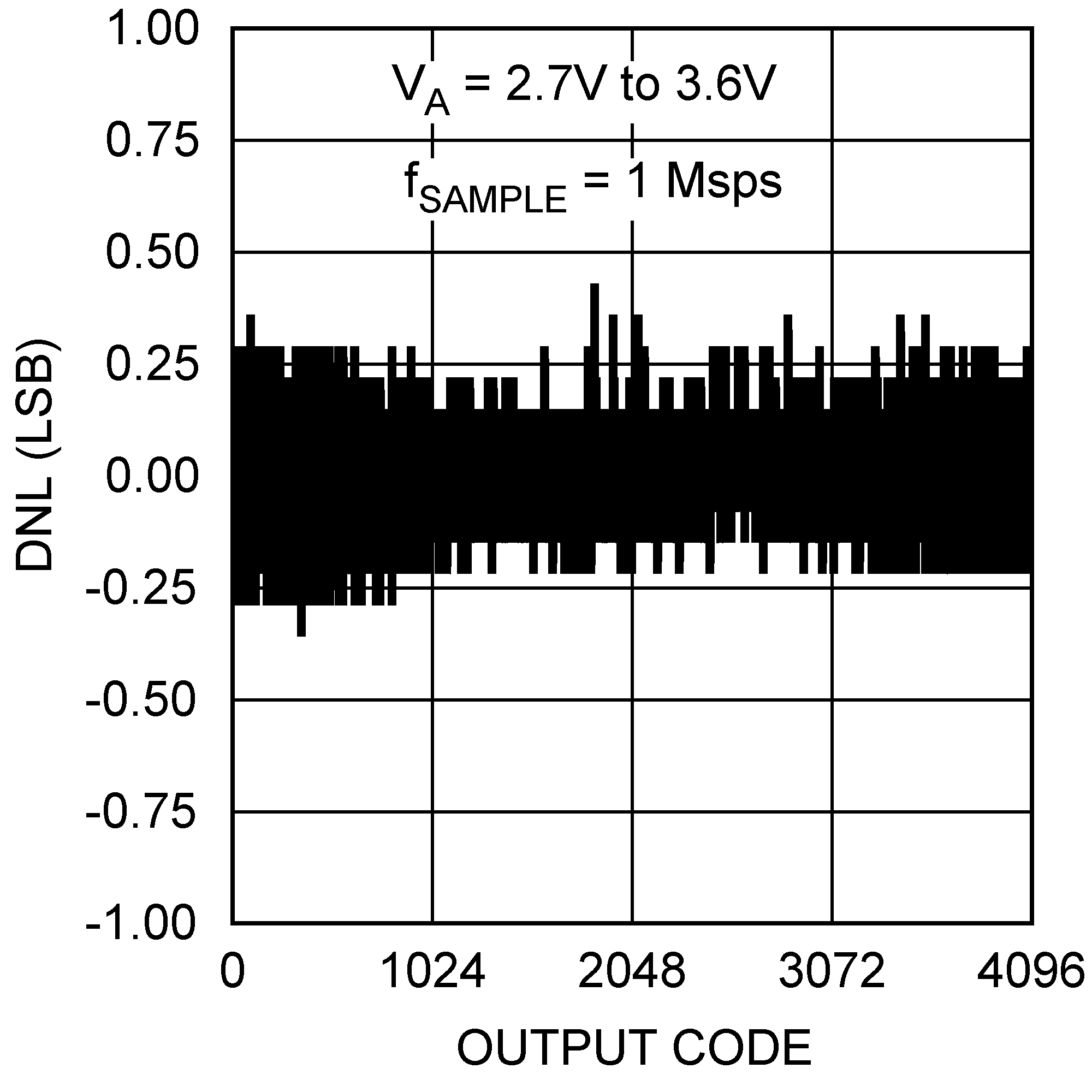 Figure 5. DNL, fSCLK = 20 MHz
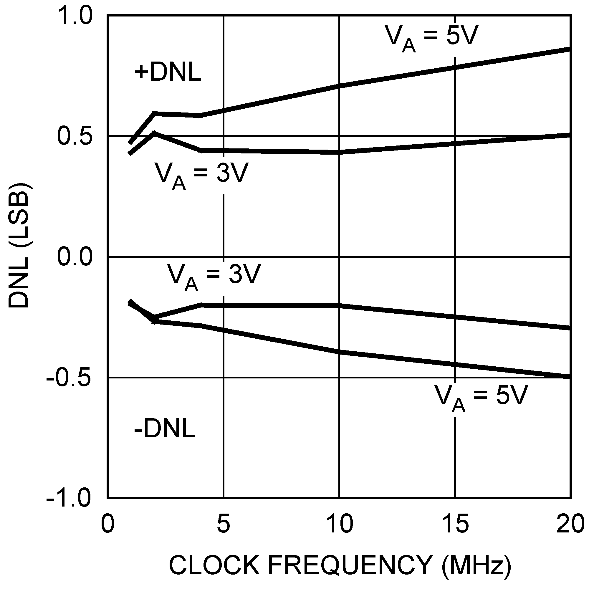 Figure 7. DNL vs Clock Frequency
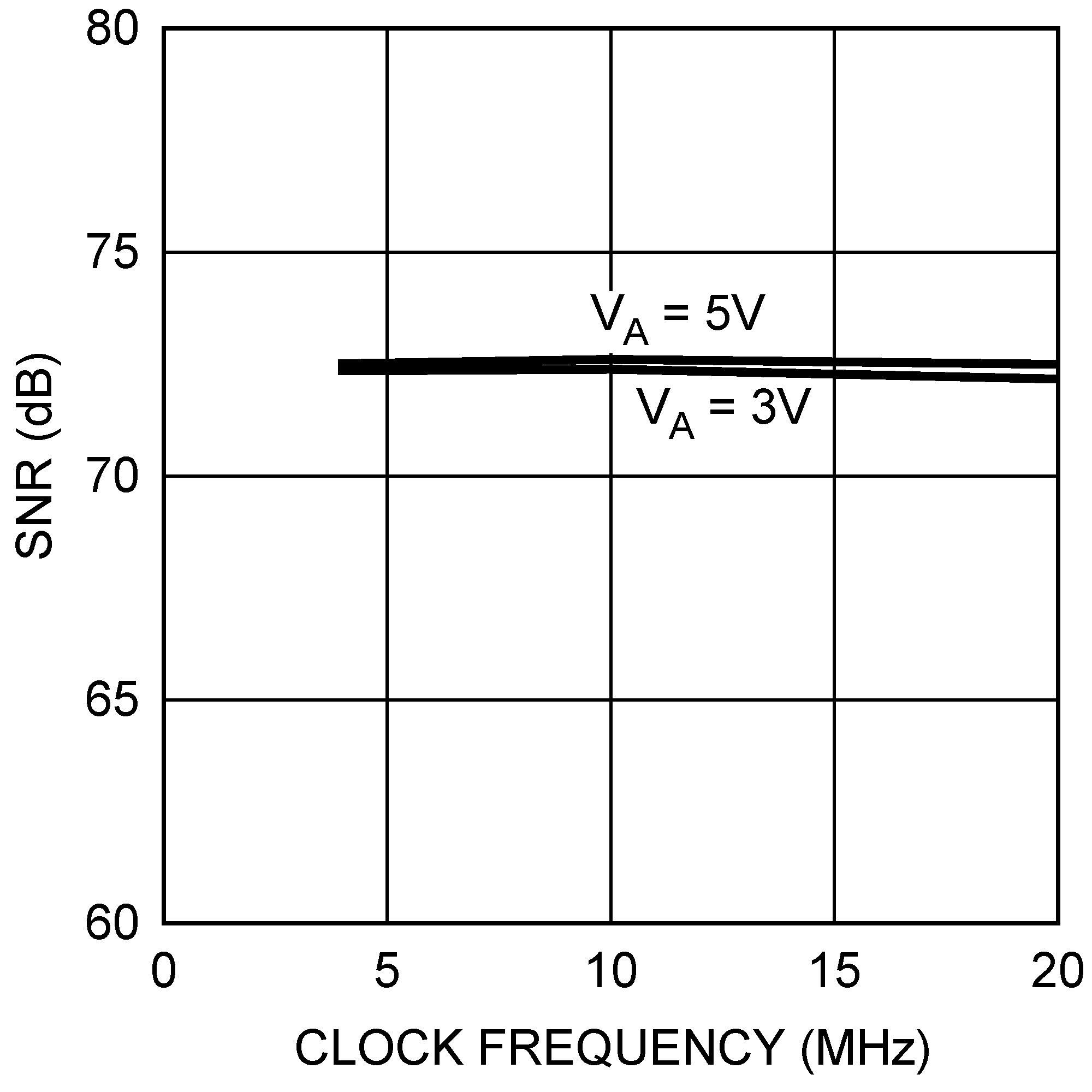 Figure 9. SNR vs Clock Frequency
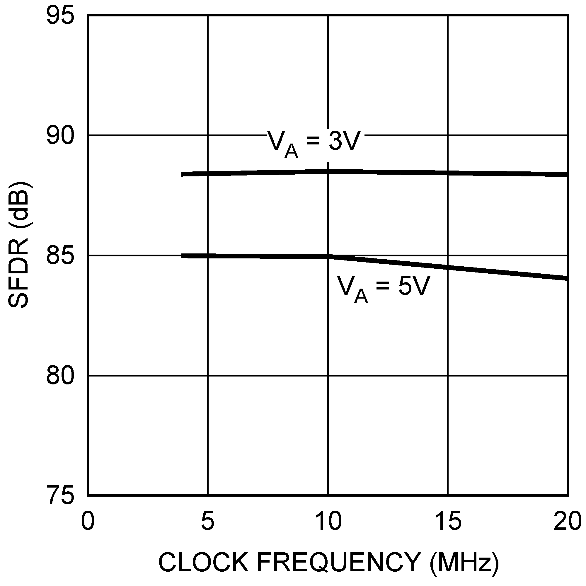 Figure 11. SFDR vs Clock Frequency
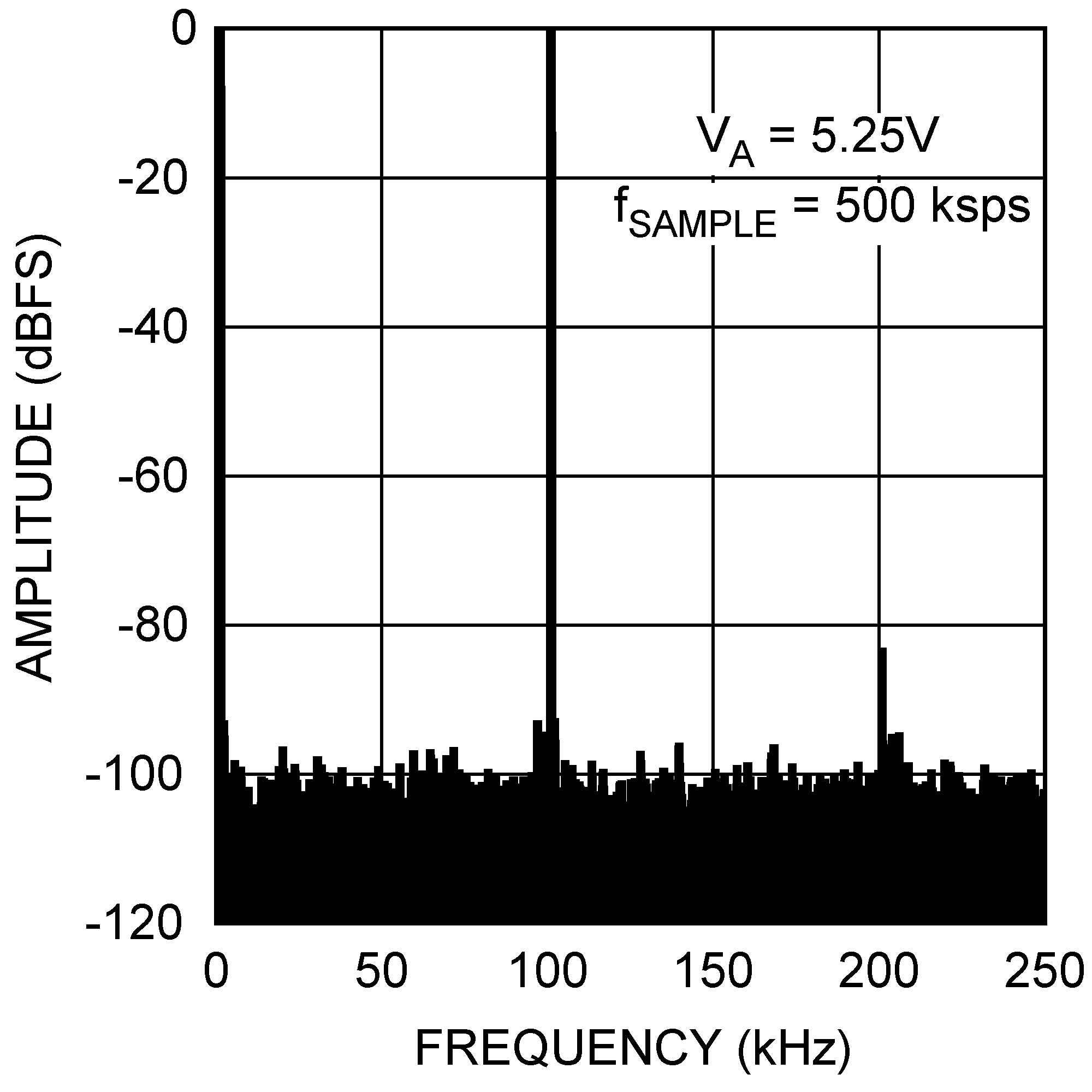 Figure 13. Spectral Response
VA = 5.25 V, fSCLK = 10 MHz
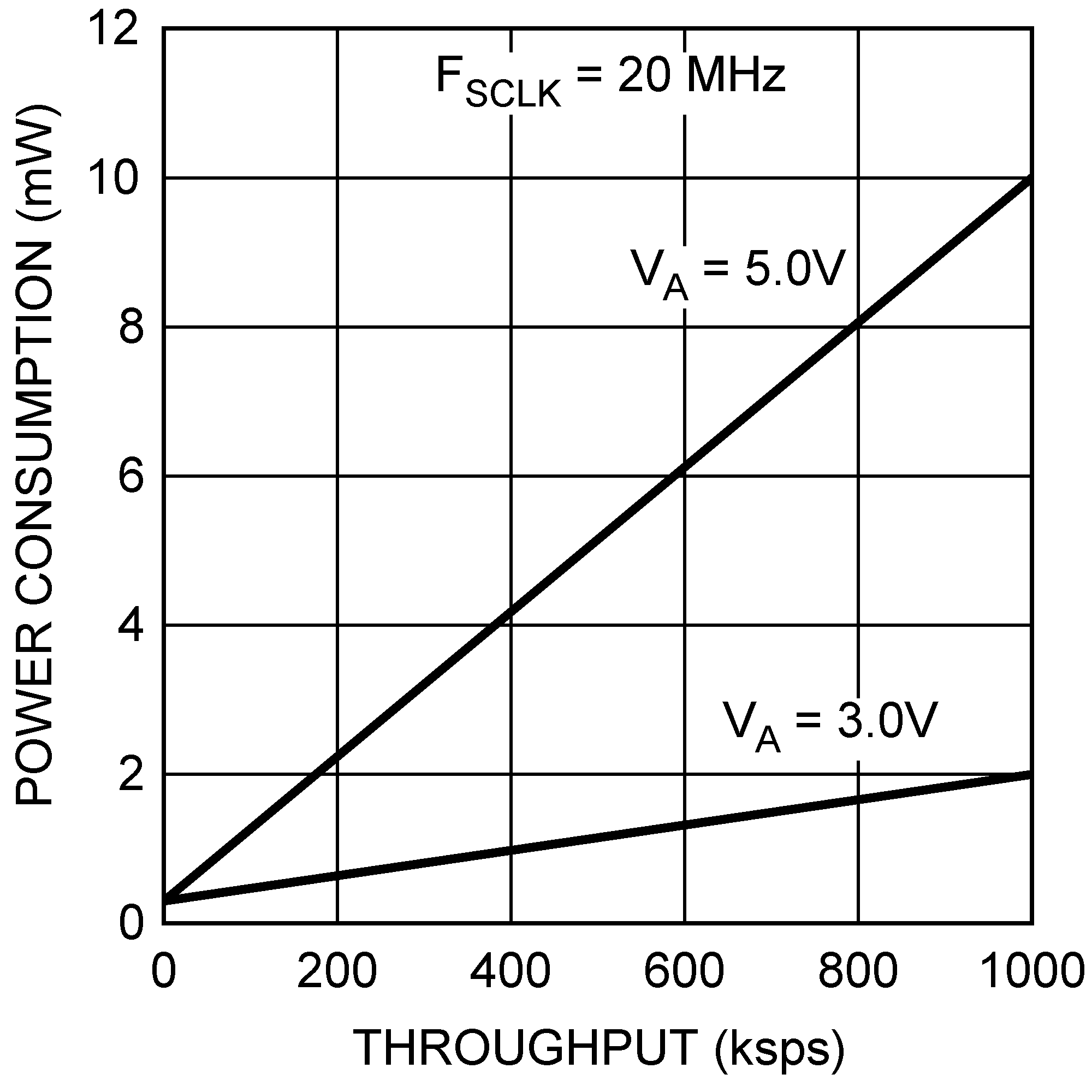 Figure 15. Power Consumption
vs Throughput, fSCLK = 20 MHz
 Figure 4. INL, fSCLK = 10 MHz
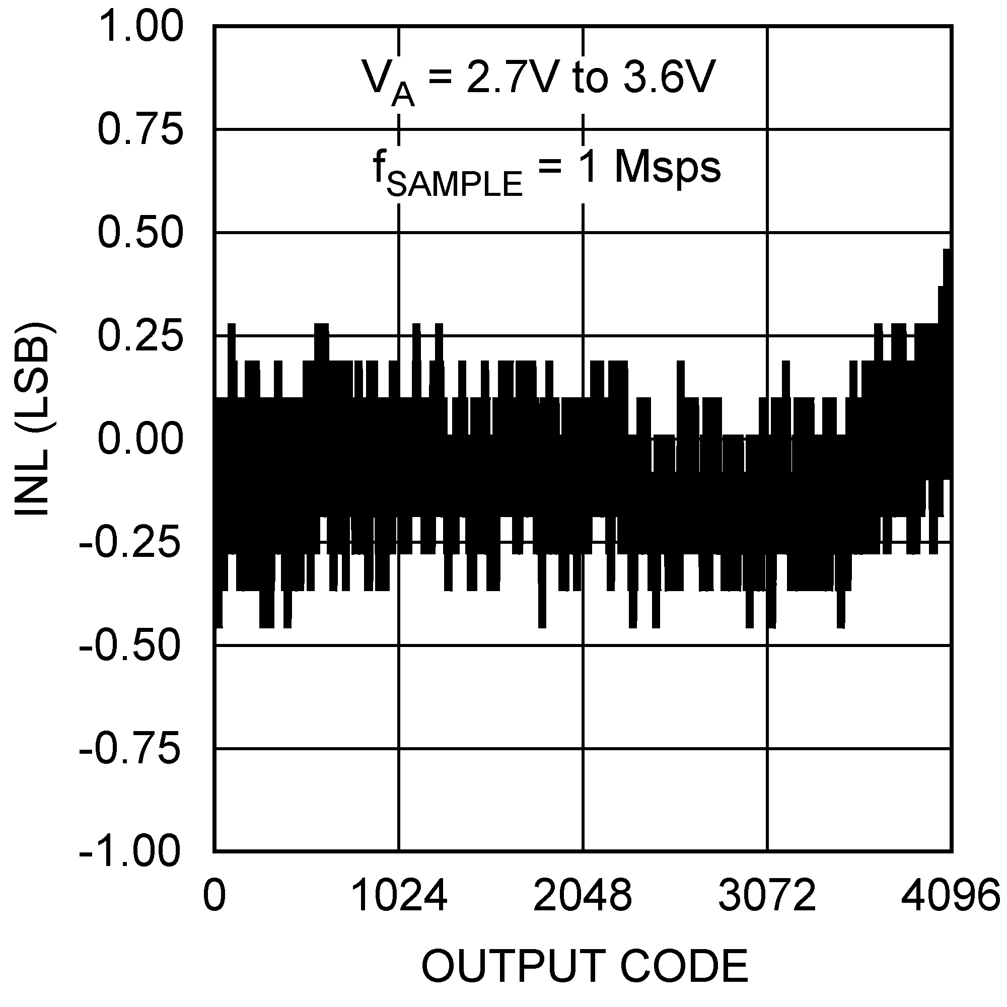 Figure 6. INL, fSCLK = 20 MHz
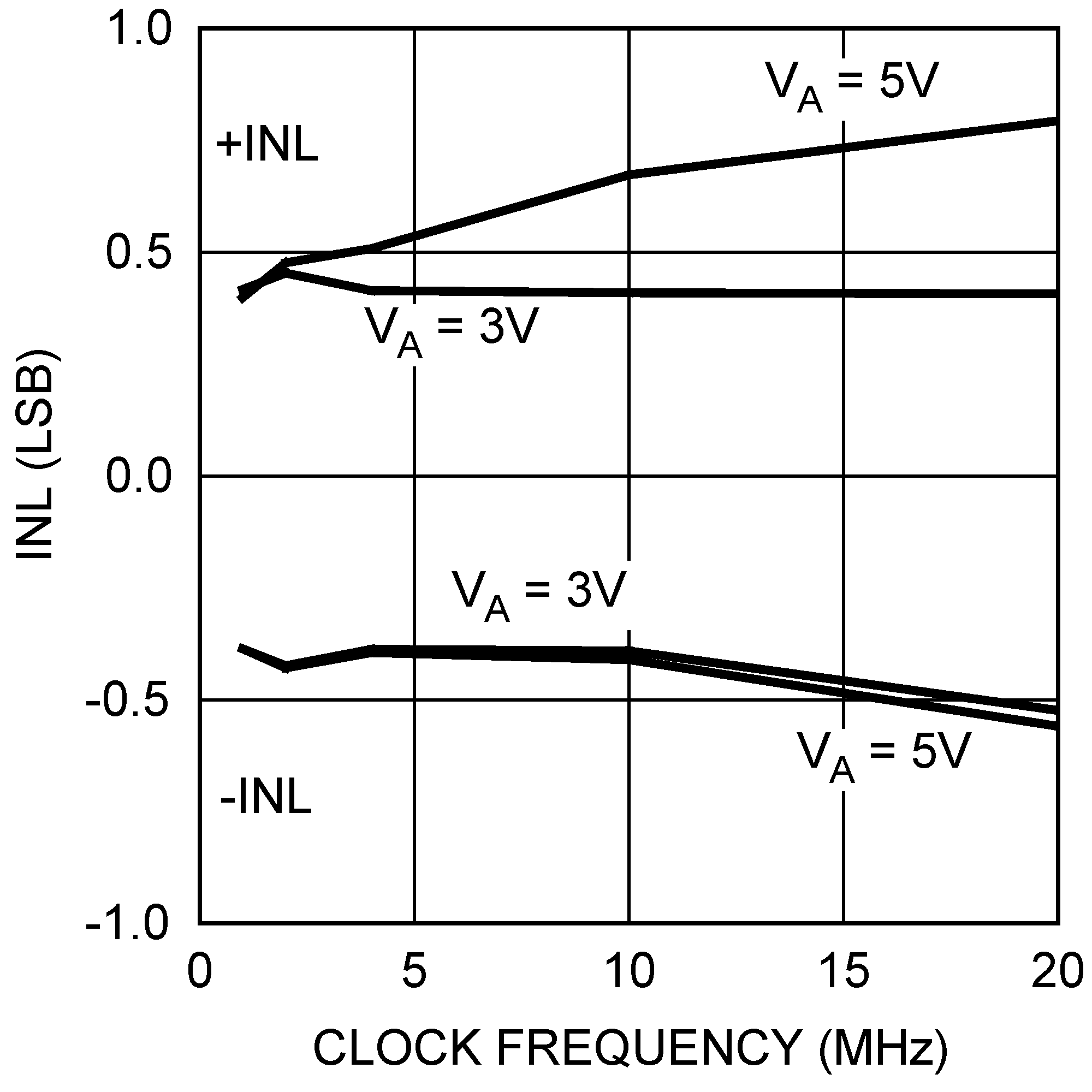 Figure 8. INL vs Clock Frequency
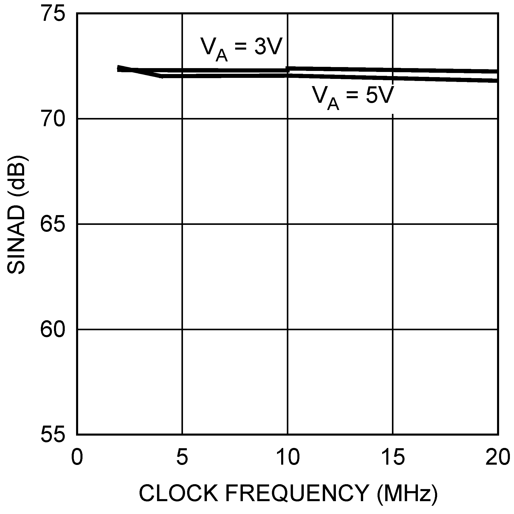 Figure 10. SINAD vs Clock Frequency
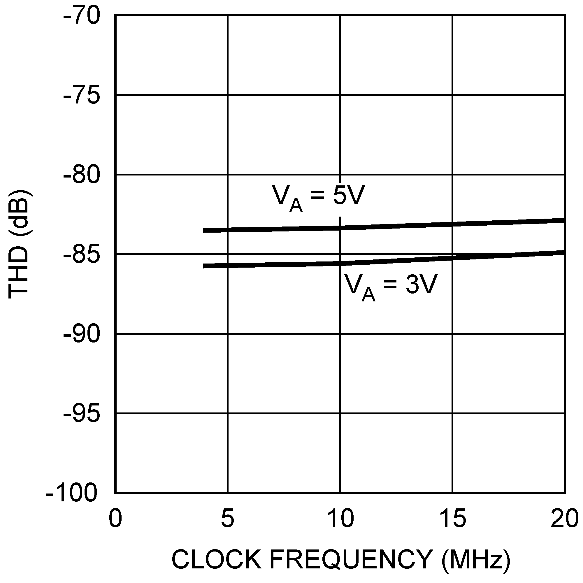 Figure 12. THD vs Clock Frequency
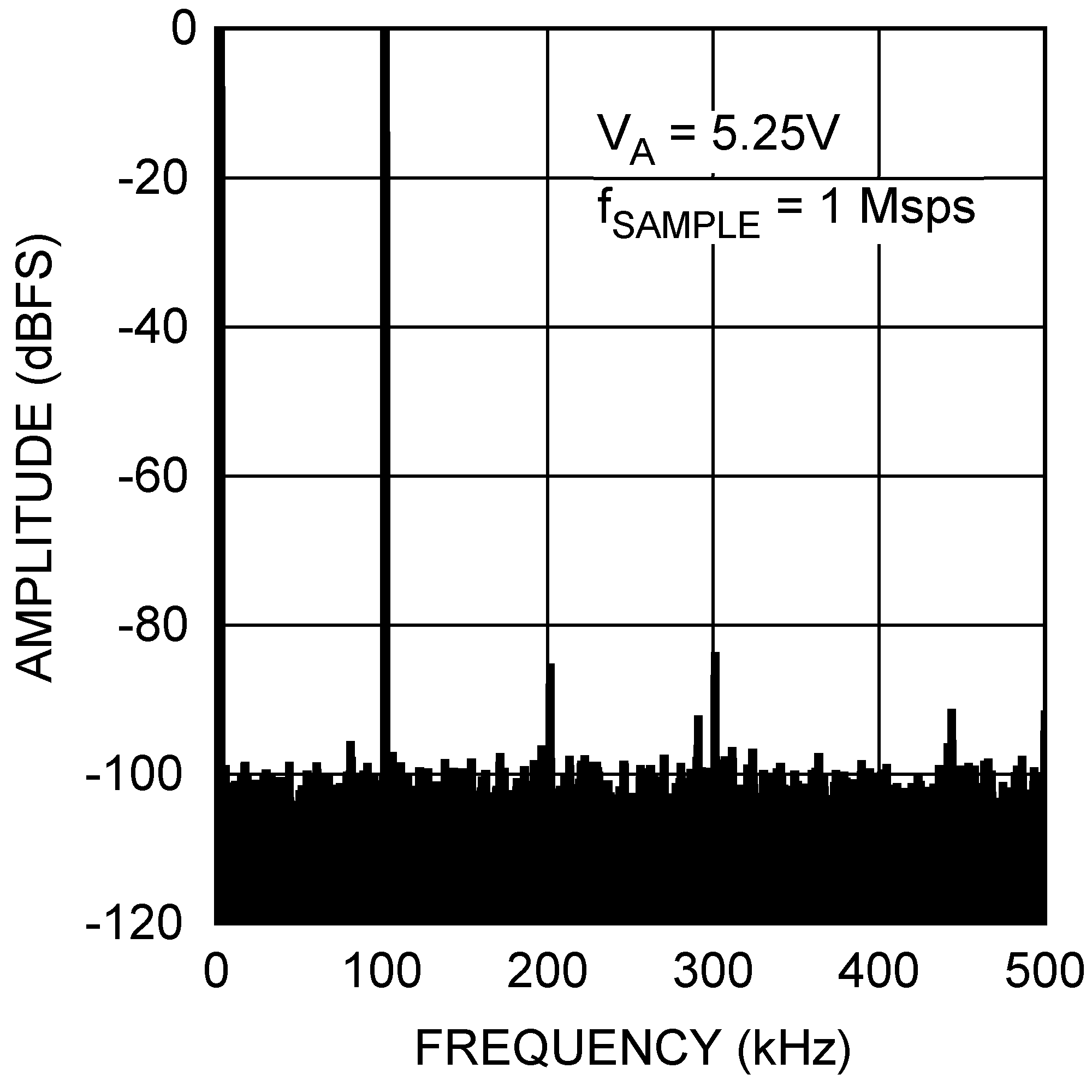 Figure 14. Spectral Response
VA = 5.25 V, fSCLK = 20 MHz