JAJSLJ3A December   2021  – April 2022 ADC128S102-SEP

PRODUCTION DATA  

  1. 特長
  2. アプリケーション
  3. 概要
  4. Revision History
  5. Pin Configuration and Functions
  6. Specifications
    1. 6.1 Absolute Maximum Ratings
    2. 6.2 ESD Ratings
    3. 6.3 Recommended Operating Conditions
    4. 6.4 Thermal Information
    5. 6.5 Electrical Characteristics
    6. 6.6 Timing Requirements
    7. 6.7 Switching Characteristics
    8. 6.8 Timing Diagrams
    9. 6.9 Typical Characteristics
  7. Detailed Description
    1. 7.1 Overview
    2. 7.2 Functional Block Diagram
    3. 7.3 Feature Description
      1. 7.3.1 ADC128S102-SEP Transfer Function
      2. 7.3.2 Analog Inputs
      3. 7.3.3 Digital Inputs and Outputs
      4. 7.3.4 Radiation Environments
        1. 7.3.4.1 Total Ionizing Dose
        2. 7.3.4.2 Single Event Latch-Up
    4. 7.4 Device Functional Modes
      1. 7.4.1 ADC128S102-SEP Operation
    5. 7.5 Programming
      1. 7.5.1 Serial Interface
  8. Application and Implementation
    1. 8.1 Application Information
    2. 8.2 Typical Application
      1. 8.2.1 Design Requirements
      2. 8.2.2 Detailed Design Procedure
      3. 8.2.3 Application Curve
  9. Power Supply Recommendations
    1. 9.1 Power-Supply Sequence
    2. 9.2 Power Management
    3. 9.3 Power-Supply Noise Considerations
  10. 10Layout
    1. 10.1 Layout Guidelines
    2. 10.2 Layout Example
  11. 11Device and Documentation Support
    1. 11.1 Receiving Notification of Documentation Updates
    2. 11.2 サポート・リソース
    3. 11.3 Trademarks
    4. 11.4 Electrostatic Discharge Caution
    5. 11.5 Glossary
  12. 12Mechanical, Packaging, and Orderable Information
    1. 12.1 Engineering Samples

パッケージ・オプション

メカニカル・データ(パッケージ|ピン)
サーマルパッド・メカニカル・データ
発注情報

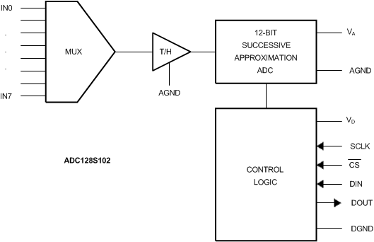
Functional Block Diagram

GUID-9BB288CE-ACA1-4A0C-BF7A-107BB6436A03-low.gif