JAJSIL5B February 2020 – October 2024 ADC12DJ1600-Q1 , ADC12QJ1600-Q1 , ADC12SJ1600-Q1
PRODUCTION DATA
- 1
- 1 特長
- 2 アプリケーション
- 3 概要
- 4 Pin Configuration and Functions
-
5 Specifications
- 5.1 Absolute Maximum Ratings
- 5.2 ESD Ratings
- 5.3 Recommended Operating Conditions
- 5.4 Thermal Information
- 5.5 Electrical Characteristics: DC Specifications
- 5.6 ADC12xJ1600-Q1: Electrical Characteristics: Power Consumption
- 5.7 ADC12xJ1600-Q1: Electrical Characteristics: AC Specifications
- 5.8 Timing Requirements
- 5.9 Switching Characteristics
- 5.10 Typical Characteristics
-
6 Detailed Description
- 6.1 Overview
- 6.2 Functional Block Diagram
- 6.3
Feature Description
- 6.3.1 Device Comparison
- 6.3.2 Analog Input
- 6.3.3 Temperature Monitoring Diode
- 6.3.4 Timestamp
- 6.3.5 Clocking
- 6.3.6
JESD204C Interface
- 6.3.6.1 Transport Layer
- 6.3.6.2 Scrambler
- 6.3.6.3 Link Layer
- 6.3.6.4 8B/10B Link Layer
- 6.3.6.5 64B/66B Link Layer
- 6.3.6.6 Physical Layer
- 6.3.6.7 JESD204C Enable
- 6.3.6.8 Multi-Device Synchronization and Deterministic Latency
- 6.3.6.9 Operation in Subclass 0 Systems
- 6.3.6.10 Alarm Monitoring
- 6.4
Device Functional Modes
- 6.4.1 Low Power Mode and High Performance Mode
- 6.4.2 JESD204C Modes
- 6.4.3 Power-Down Modes
- 6.4.4 Test Modes
- 6.4.5 Calibration Modes and Trimming
- 6.4.6 Offset Calibration
- 6.4.7 Trimming
- 6.5 Programming
- 7 Application and Implementation
- 8 Device and Documentation Support
- 9 Revision History
- 10Mechanical, Packaging, and Orderable Information
6.3.6 JESD204C Interface
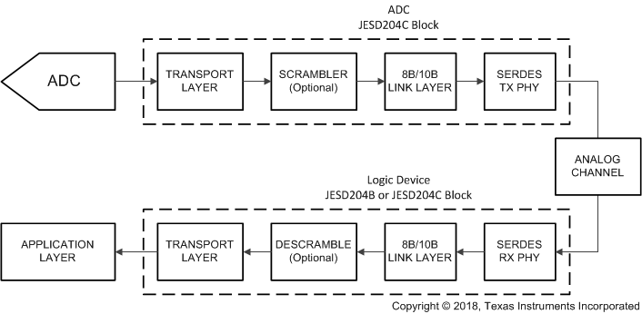
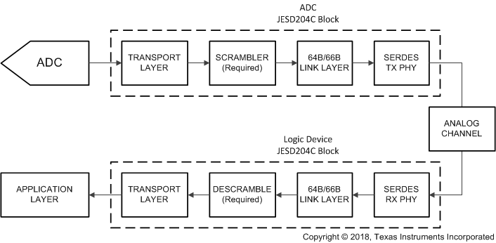
The device uses a JESD204C high-speed serial interface for data converters to transfer data from the ADC to the receiving logic device. The device serialized lanes are capable of operating with both 8B/10B encoding and 64B/66B encoding. The JESD204C output formats using 8B/10B encoding are backwards compatible with existing JESD204B receivers. A maximum of 8 lanes can be used to lower lane rates for interfacing with speed-limited logic devices. There are a few differences between 8B/10B and 64B/66B encoded JESD204C, which is highlighted throughout this section. Figure 6-7 shows a simplified block diagram of the 8B/10B encoded JESD204C interface and Figure 6-8 shows a simplified block diagram of the 64B/66B encoded JESD204C interface.
 Figure 6-7 Simplified 8B/10B Encoded JESD204C Interface Diagram
 Figure 6-8 Simplified 64B/66B Encoded JESD204C Interface Diagram
The various signals used in the JESD204C interface and the associated ADC12QJ1600-Q1 pin names are summarized briefly in Table 6-8 for reference. Most of the signals are common between 8B/10B and 64B/66B encoded JESD204C, except for SYNC which is not needed to achieve block synchronization for 64B/66B encoding. The sync header encoded into the data stream is used for block synchronization instead of the SYNC signal.
| SIGNAL NAME | PIN NAMES | 8B/10B | 64B/66B | DESCRIPTION |
|---|---|---|---|---|
| Data | Quad/dual channel: D[7:0]+, D[7:0]– Single channel: D[3:0]+, D[3:0]– | Yes | Yes | High-speed serialized data after 8B/10B or 64B/66B encoding |
| SYNC | SYNCSE | Yes | No | Link initialization signal (handshake), toggles low to start code group synchronization (CGS) process. Not used for 64B/66B encoding modes, unless it is used for NCO synchronization purposes. |
| Device clock | CLK+, CLK– or SE_CLK | Yes | Yes | ADC sampling clock or PLL reference clock, also used for clocking digital logic and output serializers |
| SYSREF | SYSREF+, SYSREF– | Yes | Yes | System timing reference used to deterministically reset the internal local multiframe clock (LMFC) or local extended multiblock clock (LEMC) counters in each JESD204C device |
Not all optional features of JESD204C are supported by ADC12QJ1600-Q1. The list of features that are supported and the features that are not supported is provided in Table 6-9.
| LETTER IDENTIFIER | REFERENCE CLAUSE | FEATURE | SUPPORT IN ADC12QJ1600-Q1 |
|---|---|---|---|
| a | clause 8 | 8B/10B link layer | Supported |
| b | clause 7 | 64B/66B link layer | Supported |
| c | clause 7 | 64B/80B link layer | Not supported |
| d | clause 7 | The command channel when using the 64B/66B or 64B/80B link layer | Not supported |
| e | clause 7 | Forward error correction (FEC) when using the 64B/66B or 64B/80B link layer | Supported |
| f | clause 7 | CRC3 when using the 64B/66B or 64B/80B link layer | Not supported |
| g | clause 8 | A physical SYNC pin when using the 8B/10B link layer | Supported |
| h | clause 7, clause 8 | Subclass 0 | Not supported, but subclass 1 transmitter is compatible with subclass 0 receiver |
| i | clause 7, clause 8 | Subclass 1 | Supported |
| j | clause 8 | Subclass 2 | Not supported |
| k | clause 7, clause 8 | Lane alignment within a single link | Supported |
| l | clause 7, clause 8 | Subclass 1 with support for a lane alignment on a multipoint link by means of the MULTIREF signal | Not supported |
| m | clause 8 | SYNC interface timing is compatible with JESD204A | Supported |
| n | clause 8 | SYNC interface timing is compatible with JESD204B | Supported |