SLASE49B December 2015 – April 2017 ADC14X250
PRODUCTION DATA.
- 1 Features
- 2 Applications
- 3 Description
- 4 Revision History
- 5 Pin Configuration and Functions
-
6 Specifications
- 6.1 Absolute Maximum Ratings
- 6.2 ESD Ratings
- 6.3 Recommended Operating Conditions
- 6.4 Thermal Information
- 6.5 Electrical Characteristics: Static Converter Performance
- 6.6 Electrical Characteristics: Dynamic Converter Performance
- 6.7 Electrical Characteristics: Power Supply
- 6.8 Electrical Characteristics: Analog Interface
- 6.9 Digital Input Characteristics
- 6.10 Electrical Characteristics: Serial Data Output Interface
- 6.11 Electrical Characteristics: Digital Input
- 6.12 Timing Requirements
- 6.13 Typical Characteristics
- 7 Parameter Measurement Information
-
8 Detailed Description
- 8.1 Overview
- 8.2 Functional Block Diagram
- 8.3
Feature Description
- 8.3.1 Amplitude and Phase Imbalance Correction of Differential Analog Input
- 8.3.2 Input Clock Divider
- 8.3.3 SYSREF Offset Feature and Detection Gate
- 8.3.4 DC Offset Correction
- 8.3.5 Serial Differential Output Drivers
- 8.3.6 ADC Core Calibration
- 8.3.7 Data Format
- 8.3.8 JESD204B Supported Features
- 8.3.9 Transport Layer Configuration
- 8.3.10 Test Pattern Sequences
- 8.3.11 JESD204B Link Initialization
- 8.3.12 Sync~ Signal Selection
- 8.3.13 SPI
- 8.4 Device Functional Modes
- 8.5
Register Map
- 8.5.1
Register Descriptions
- 8.5.1.1 CONFIG_A, [Address: 0x0000], [Default: 0x3C]
- 8.5.1.2 DEVICE CONFIG, [Address: 0x0002], [Default: 0x00]
- 8.5.1.3 CHIP_TYPE, [Address: 0x0003], [Default: 0x03]
- 8.5.1.4 CHIP_ID, [Address: 0x0005, 0x0004], [Default: 0x00, 0x01]
- 8.5.1.5 CHIP_VERSION, [Address: 0x0006], [Default: 0x00]
- 8.5.1.6 VENDOR_ID, [Address: 0x000D, 0x000C], [Default: 0x04, 0x51]
- 8.5.1.7 SPI_CFG, [Address: 0x0010], [Default: 0x01]
- 8.5.1.8 OM1 (Operational Mode 1), [Address: 0x0012], [Default: 0x81]
- 8.5.1.9 OM2 (Operational Mode 2), [Address: 0x0013], [Default: 0x20]
- 8.5.1.10 IMB_ADJ (Imbalance Adjust), [Address: 0x0014], [Default: 0x00]
- 8.5.1.11 DC_MODE (DC Offset Correction Mode), [Address: 0x003D], [Default: 0x00]
- 8.5.1.12 SER_CFG (Serial Lane Transmitter Configuration), [Address: 0x0047], [Default: 0x00]
- 8.5.1.13 JESD_CTRL1 (JESD Configuration Control 1) , [Address: 0x0060], [Default: 0x7D]
- 8.5.1.14 JESD_CTRL2 (JESD Configuration Control 2), [Address: 0x0061], [Default: 0x00]
- 8.5.1.15 JESD_RSTEP (JESD Ramp Pattern Step), [Addresses: 0x0063, 0x0062], [Default: 0x00, 0x01]
- 8.5.1.16 JESD_STATUS (JESD Link Status), [Address: 0x006C], [Default: N/A]
- 8.5.1
Register Descriptions
- 9 Application and Implementation
- 10Power Supply Recommendations
- 11Layout
- 12Device and Documentation Support
- 13Mechanical, Packaging, and Orderable Information
パッケージ・オプション
メカニカル・データ(パッケージ|ピン)
- RHB|32
サーマルパッド・メカニカル・データ
- RHB|32
発注情報
1 Features
- Resolution: 14-Bit
- Conversion Rate: 250 MSPS
- Performance:
- Input: 240 MHz, –3 dBFS
- SNR: 70.1 dBFS
- Noise Spectral Density: –151.1 dBFS/Hz
- SFDR: 87 dBFS
- Non-HD2 and Non-HD3 SPUR: –92 dBFS
- No Input SNR: 71.1 dBFS
- Input: 240 MHz, –3 dBFS
- Power Dissipation: 584 mW
- Performance Rated up to 105°C (at thermal pad)
- JESD204B Subclass 1 Single Lane Serial Data Interface With Lane Rate Up To 5 Gb/s
- Buffered Analog Inputs
- Differential Input Phase and Amplitude Correction
- Input Sampling Clock Divider (Divide-by-1,2,4,8)
- 4-Wire Serial Peripheral Interface (SPI)
- 32-Pin WQFN Package (5×5 mm, 0.5-mm Pitch)
2 Applications
- High IF Sampling Receivers
- Multi-Carrier Base Station Receivers
- GSM/EDGE, CDMA2000, UMTS, LTE, WiMax
- Diversity, Multi-Mode, and Multiband Receivers
- Digital Pre-Distortion
- Software Defined Radio (SDR)
- Test and Measurement Equipment
- Communications Instrumentation
- Radar
- Portable Instrumentation
3 Description
The ADC14X250 device is a monolithic single-channel high performance analog-to-digital converter capable of converting analog input signals into 14-bit digital words with a sampling rate of 250 MSPS. This converter uses a differential pipelined architecture with integrated input buffer to provide excellent dynamic performance and low power consumption across an extended temperature range from –40°C to 105°C as measured at the device's PCB footprint thermal pad.
The integrated input buffer eliminates charge kickback noise coming from the internal switched capacitor sampling circuits and eases the system-level design of the driving amplifier, anti-aliasing filter, and impedance matching. The buffer can be also be adjusted to correct for phase and amplitude imbalance of the differential input signal path to improve even order harmonic distortion. An input sampling clock divider provides integer divide ratios to simplify system clocking. An integrated low-noise voltage reference eases board level design without requiring external decoupling capacitors. The output digital data is provided through a JESD204B subclass 1 single lane interface from a 32-pin, 5-mm × 5-mm WQFN package. The ADC14X250 operates on 1.2 V, 1.8 V and 3.0 V power supplies. A SPI is available to configure the device that is compatible with 1.2-V to 3-V logic.
Device Information(1)
| PART NAME | PACKAGE | BODY SIZE (NOM) |
|---|---|---|
| ADC14X250 | WQFN (32) | 5.00 × 5.00 mm |
- For all available packages, see the orderable addendum at the end of the data sheet.
SPACE
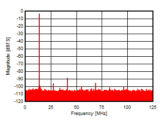
1-Tone Spectrum, Input 240 MHz –3 dBFS

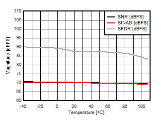
Performance Stability Across
Temperature (240 MHz)
