SLASE49B December 2015 – April 2017 ADC14X250
PRODUCTION DATA.
- 1 Features
- 2 Applications
- 3 Description
- 4 Revision History
- 5 Pin Configuration and Functions
-
6 Specifications
- 6.1 Absolute Maximum Ratings
- 6.2 ESD Ratings
- 6.3 Recommended Operating Conditions
- 6.4 Thermal Information
- 6.5 Electrical Characteristics: Static Converter Performance
- 6.6 Electrical Characteristics: Dynamic Converter Performance
- 6.7 Electrical Characteristics: Power Supply
- 6.8 Electrical Characteristics: Analog Interface
- 6.9 Digital Input Characteristics
- 6.10 Electrical Characteristics: Serial Data Output Interface
- 6.11 Electrical Characteristics: Digital Input
- 6.12 Timing Requirements
- 6.13 Typical Characteristics
- 7 Parameter Measurement Information
-
8 Detailed Description
- 8.1 Overview
- 8.2 Functional Block Diagram
- 8.3
Feature Description
- 8.3.1 Amplitude and Phase Imbalance Correction of Differential Analog Input
- 8.3.2 Input Clock Divider
- 8.3.3 SYSREF Offset Feature and Detection Gate
- 8.3.4 DC Offset Correction
- 8.3.5 Serial Differential Output Drivers
- 8.3.6 ADC Core Calibration
- 8.3.7 Data Format
- 8.3.8 JESD204B Supported Features
- 8.3.9 Transport Layer Configuration
- 8.3.10 Test Pattern Sequences
- 8.3.11 JESD204B Link Initialization
- 8.3.12 Sync~ Signal Selection
- 8.3.13 SPI
- 8.4 Device Functional Modes
- 8.5
Register Map
- 8.5.1
Register Descriptions
- 8.5.1.1 CONFIG_A, [Address: 0x0000], [Default: 0x3C]
- 8.5.1.2 DEVICE CONFIG, [Address: 0x0002], [Default: 0x00]
- 8.5.1.3 CHIP_TYPE, [Address: 0x0003], [Default: 0x03]
- 8.5.1.4 CHIP_ID, [Address: 0x0005, 0x0004], [Default: 0x00, 0x01]
- 8.5.1.5 CHIP_VERSION, [Address: 0x0006], [Default: 0x00]
- 8.5.1.6 VENDOR_ID, [Address: 0x000D, 0x000C], [Default: 0x04, 0x51]
- 8.5.1.7 SPI_CFG, [Address: 0x0010], [Default: 0x01]
- 8.5.1.8 OM1 (Operational Mode 1), [Address: 0x0012], [Default: 0x81]
- 8.5.1.9 OM2 (Operational Mode 2), [Address: 0x0013], [Default: 0x20]
- 8.5.1.10 IMB_ADJ (Imbalance Adjust), [Address: 0x0014], [Default: 0x00]
- 8.5.1.11 DC_MODE (DC Offset Correction Mode), [Address: 0x003D], [Default: 0x00]
- 8.5.1.12 SER_CFG (Serial Lane Transmitter Configuration), [Address: 0x0047], [Default: 0x00]
- 8.5.1.13 JESD_CTRL1 (JESD Configuration Control 1) , [Address: 0x0060], [Default: 0x7D]
- 8.5.1.14 JESD_CTRL2 (JESD Configuration Control 2), [Address: 0x0061], [Default: 0x00]
- 8.5.1.15 JESD_RSTEP (JESD Ramp Pattern Step), [Addresses: 0x0063, 0x0062], [Default: 0x00, 0x01]
- 8.5.1.16 JESD_STATUS (JESD Link Status), [Address: 0x006C], [Default: N/A]
- 8.5.1
Register Descriptions
- 9 Application and Implementation
- 10Power Supply Recommendations
- 11Layout
- 12Device and Documentation Support
- 13Mechanical, Packaging, and Orderable Information
パッケージ・オプション
メカニカル・データ(パッケージ|ピン)
- RHB|32
サーマルパッド・メカニカル・データ
- RHB|32
発注情報
6 Specifications
6.1 Absolute Maximum Ratings
over operating free-air temperature range (unless otherwise noted) (1)| MIN | MAX | UNIT | ||
|---|---|---|---|---|
| Supply Voltage | VA3.0 | –0.3 | 4.2 | V |
| VA1.8 | –0.3 | 2.35 | V | |
| VA1.2 | –0.3 | 1.55 | V | |
| Voltage at: | VIN+, VIN– | VCM – 0.75(4) | VCM + 0.75 | V |
| VCM | –0.3 | VA3.0 + 0.3, not to exceed 4.2 V | V | |
| SCLK, SDI, CSb | –0.3 | VA3.0 + 0.3, not to exceed 4.2 V | V | |
| SDO | –0.3 | VSPI + 0.3, not to exceed 4.2 V | V | |
| CLKIN+, CLKIN–, SYSREF+, SYSREF– | –0.3 | 1.55 | V | |
| SYNC+, SYNC– | –0.3 | VBP2.5 + 0.3 | V | |
| BP2.5 | –0.3 | 3.2 | V | |
| SO+, SO– | –0.3 | VBP2.5 + 0.3 | V | |
| Input current at any pin(3) | 5 | mA | ||
| TJ | Operating junction temperature(2) | 125 | °C | |
| Tstg | Storage temperature range | –65 | 150 | °C |
(1) Stresses beyond those listed under Absolute Maximum Ratings may cause permanent damage to the device. These are stress ratings only, which do not imply functional operation of the device at these or any other conditions beyond those indicated under Recommended Operating Conditions. Exposure to absolute-maximum-rated conditions for extended periods may affect device reliability.
(2) Prolonged use at this temperature may increase the device failure-in-time (FIT) rate.
(3) When the input voltage at any pin exceeds the VA3.0 power supply (that is VIN > VA3.0 or VIN < AGND) the current at that pin should be limited to ±5 mA. The ±50-mA maximum package input current rating limits the number of pins that can safely exceed the power supplies with an input current of ±5 mA to 10 pins.
(4) VCM refers to the voltage bias present at the VCM output. The Absolute Maximum Rating for the VIN+ and VIN– inputs may extend down to –0.3V for the purpose of the initial power-up transient only. Forcing these pins to a voltage lower than VCM – 0.75 for an extended time may reduce the operating lifetime of the device.
6.2 ESD Ratings
| VALUE | UNIT | |||
|---|---|---|---|---|
| V(ESD) | Electrostatic discharge | Human body model (HBM), per ANSI/ESDA/JEDEC JS-001(1) | ±2500 | V |
| Charged device model (CDM), per JEDEC specification JESD22-C101(2) | ±1000 | |||
(1) JEDEC document JEP155 states that 500-V HBM allows safe manufacturing with a standard ESD control process.
(2) JEDEC document JEP157 states that 250-V CDM allows safe manufacturing with a standard ESD control process.
6.3 Recommended Operating Conditions
Operation of the device beyond the recommended operating ratings is not recommended as it may degrade the device lifetime.| MIN | MAX | UNIT | ||
|---|---|---|---|---|
| TA-MIN | Specified temperature minimum, ambient air. | –40 | °C | |
| TA-MAX | Specified temperature maximum, ambient air.(1) | 85 | °C | |
| TP-MAX | Specified temperature maximum, measured at the device's footprint thermal pad on the printed circuit board. | 105 | °C | |
| TJ | Operating junction temperature(2) | 106 | °C | |
(1) This device may be operated above the maximum ambient temperature (TA-MAX) up to the value of TP-MAX as long as the maximum temperature at the device's footprint thermal pad on the printed circuit board remains less than TP-MAX.
(2) The recommended maximum operating junction temperature assumes the junction to package bottom thermal resistance, RθJC(bottom) = 1.1°C/W, the thermal resistance of the device thermal pad connection to the PCB footprint is negligible, and the recommended maximum temperature at the PCB footprint thermal pad, TP-MAX, is satisfied.
6.4 Thermal Information
| THERMAL METRIC(1) | RHB (WQFN) | UNIT | |
|---|---|---|---|
| (32 PINS) | |||
| RθJA | Thermal resistance, junction to ambient | 31.4 | °C/W |
| RθJC(top) | Thermal resistance, junction to package top | 50.2 | |
| RθJC(bottom) | Thermal resistance, junction to package bottom | 1.1 | |
| RθJB | Thermal resistance, junction to board | 5.1 | |
| φJT | Characterization parameter, junction to package top | 0.2 | |
| φJB | Characterization parameter, junction to board | 5.1 | |
(1) For more information about traditional and new thermal metrics, see the Semiconductor and IC Package Thermal Metrics application report.
6.5 Electrical Characteristics: Static Converter Performance
Unless otherwise noted, these specifications apply for VA3.0 = 3 V; VA1.8 = 1.8 V; VA1.2 = 1.2 V; FCLKIN = FS = 250 MSPS; external differential resistive termination at ADC input is 66 Ω. Typical values are at TA = 25°C, unless otherwise noted. Limit values specified for the temperature range TA-MIN = –40°C to TP-MAX = 105°C.| PARAMETER | TEST CONDITIONS | MIN | TYP | MAX | UNIT | |
|---|---|---|---|---|---|---|
| RESOLUTION | Bit resolution of ADC core | 14 | Bits | |||
| FSR | Full scale range Differential peak-to-peak |
1.7 | Vpp | |||
| GVAR | Gain variation 1-sigma variation of full scale range across multiple units |
±0.05 | dB | |||
| VOFF | Input referred voltage offset | ±3 | mV | |||
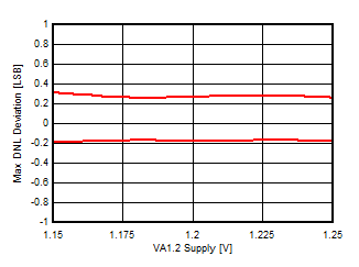
| DNL | Differential non-linearity | +0.27 –0.18 |
LSB | |||
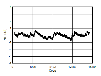
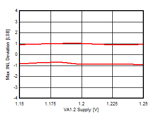
| INL | Integral non-linearity | +1 –0.9 |
LSB | |||
6.6 Electrical Characteristics: Dynamic Converter Performance
Unless otherwise noted, these specifications apply for VA3.0 = 3 V; VA1.8 = 1.8 V; VA1.2 = 1.2 V; FCLKIN = FS = 250 MSPS; external differential resistive termination at ADC input is 66 Ω. CLKIN± input is a 2 Vp-p differential sinusoid. Typical values are at TA = 25°C, unless otherwise noted. Limit values specified for the temperature range TA-MIN = –40°C to TP-MAX = 105°C.| PARAMETER | TEST CONDITIONS | MIN | TYP | MAX | UNIT | |
|---|---|---|---|---|---|---|
| BW3dB | 3-dB bandwidth Frequency at which the voltage input to digital output response deviates by 3 dB compared to low frequencies for a low impedance differential signal applied at the input pins. Includes 0.5-nH parasitic inductance in series with each pin of the differential analog input. |
800 | MHz | |||
| SNR | Signal-to-noise ratio, integrated across entire Nyquist bandwidth | dBFS | ||||
| Input = 10 MHz, –3 dBFS | 71.1 | |||||
| Input = 70 MHz, –3 dBFS | 70.9 | |||||
| Input = 170 MHz, –3 dBFS | 70.5 | |||||
| Input = 240 MHz, –3 dBFS | 68.3 | 70.1 | ||||
| Input = 240 MHz, –40 dBFS | 71.1 | |||||
| Input = 300 MHz, –3 dBFS | 69.7 | |||||
| SINAD | Signal-to-noise and distortion ratio, integrated across Nyquist bandwidth | dBFS | ||||
| Input = 10 MHz, –3 dBFS | 71.0 | |||||
| Input = 70 MHz, –3 dBFS | 70.8 | |||||
| Input = 170 MHz, –3 dBFS | 70.0 | |||||
| Input = 240 MHz, –3 dBFS | 70.0 | |||||
| Input = 240 MHz, –40 dBFS | 71.0 | |||||
| Input = 300 MHz, –3 dBFS | 69.4 | |||||
| ENOB | Signal-to-noise and distortion ratio, integrated across Nyquist bandwidth | Bits | ||||
| Input = 10 MHz, –3 dBFS | 11.5 | |||||
| Input = 70 MHz, –3 dBFS | 11.5 | |||||
| Input = 170 MHz, –3 dBFS | 11.3 | |||||
| Input = 240 MHz, –3 dBFS | 11.3 | |||||
| Input = 300 MHz, –3 dBFS | 11.2 | |||||
| NSD | Noise spectral density, average NSD across Nyquist bandwidth | dBFS/Hz | ||||
| Input = 10 MHz, –3 dBFS | –152.1 | |||||
| Input = 70 MHz, –3 dBFS | –151.9 | |||||
| Input = 170 MHz, –3 dBFS | –151.5 | |||||
| Input = 240 MHz, –3 dBFS | –151.1 | |||||
| Input = 240 MHz, –40 dBFS | –152.1 | |||||
| Input = 300 MHz, –3 dBFS | –150.7 | |||||
| SFDR | Spurious free dynamic range, single tone | dBFS | ||||
| Input = 10 MHz, –3 dBFS | 93 | |||||
| Input = 70 MHz, –3 dBFS | 92 | |||||
| Input = 170 MHz, –3 dBFS | 80 | |||||
| Input = 240 MHz, –3 dBFS | 75 | 87 | ||||
| Input = 300 MHz, –3 dBFS | 86 | |||||
| HD2 | 2nd order harmonic distortion | dBFS | ||||
| Input = 10 MHz, –3 dBFS | –95 | |||||
| Input = 70 MHz, –3 dBFS | –95 | |||||
| Input = 170 MHz, –3 dBFS | –92 | |||||
| Input = 240 MHz, –3 dBFS | –75 | –90 | ||||
| Input = 300 MHz, –3 dBFS | –90 | |||||
| HD3 | 3rd order harmonic distortion | dBFS | ||||
| Input = 10 MHz, –3 dBFS | –95 | |||||
| Input = 70 MHz, –3 dBFS | –95 | |||||
| Input = 170 MHz, –3 dBFS | –80 | |||||
| Input = 240 MHz, –3 dBFS | –75 | –87 | ||||
| Input = 300 MHz, –3 dBFS | –86 | |||||
| Non HD2, HD3 | Largest spurious tone, not including DC, HD2 or HD3 | dBFS | ||||
| Input = 10 MHz, –3 dBFS | –95 | |||||
| Input = 70 MHz, –3 dBFS | –95 | |||||
| Input = 170 MHz, –3 dBFS | –92 | |||||
| Input = 240 MHz, –3 dBFS | –80 | –92 | ||||
| Input = 300 MHz, –3 dBFS | –92 | |||||
| IMD3 | Third-order intermodulation, dual tone | dBFS | ||||
| Tone 1 = 235 MHz, –10 dBFS Tone 2 = 240 MHz, –10 dBFS |
–94 | |||||
6.7 Electrical Characteristics: Power Supply
Unless otherwise noted, these specifications apply for VA3.0 = 3 V; VA1.8 = 1.8 V; VA1.2 = 1.2 V; FCLKIN = FS = 250 MSPS. Typical values are at TA = 25°C, unless otherwise noted. Limit values specified for the temperature range TA-MIN = –40°C to TP-MAX = 105°C.| PARAMETER | TEST CONDITIONS | MIN | TYP | MAX | UNIT | ||
|---|---|---|---|---|---|---|---|
| VA3.0 | 3.0V analog voltage supply | 2.85 | 3.0 | 3.45 | V | ||
| VA1.8 | 1.8V analog voltage supply | 1.7 | 1.8 | 1.9 | V | ||
| VA1.2 | 1.2V analog voltage supply | 1.15 | 1.2 | 1.25 | V | ||
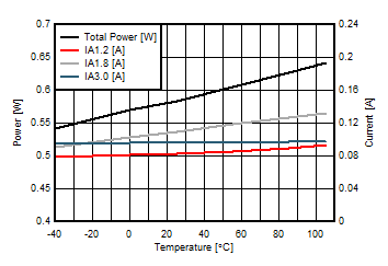
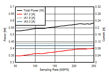
| IA3.0 | VA3.0 supply current consumption | 95 | mA | ||||
| IA1.8 | VA1.8 supply current consumption | 112 | mA | ||||
| IA1.2 | VA1.2 supply current consumption | 78 | mA | ||||
| PT | Total power consumption of the VA3.0 , VA1.8 , VA1.2 supplies(1)
|
Normal operation(2) | 584 | 600 | mW | ||
| Power consumption during power-down state, external clock active | 38 | ||||||
| Power consumption during sleep state, external clock active | 38 | ||||||
| VBP2.5 | BP2.5 bias voltage | Do not load the BP2.5 pin | 2.65 | V | |||
| Supply sensitivity to noise Power of spectral spur resulting from a 100-mV sinusoidal signal modulating a supply at 500 kHz. Analog input is a –3 dBFS 150-MHz single tone. In all cases, the spur appears as part of a pair symmetric about the fundamental that scales proportionally with the fundamental amplitude. |
dBFS | ||||||
| VA3.0 | –72.5 | ||||||
| VA1.8 | –58.0 | ||||||
| VA1.2 | –37.7 | ||||||
(1) Power values indicate consumption during normal conversion assuming an established JESD204 link.
(2) The power limit applies to an ambient temperature and board thermal pad temperature of 25°C.
6.8 Electrical Characteristics: Analog Interface
Unless otherwise noted, these specifications apply for VA3.0 = 3 V; VA1.8 = 1.8 V; VA1.2 = 1.2 V; FCLKIN = FS = 250 MSPS; external differential resistive termination at ADC input is 66 Ω. Typical values are at TA = 25°C. Limit values specified for the temperature range TA-MIN = –40°C to TP-MAX = 105°C.| PARAMETER | TEST CONDIONS | MIN | TYP | MAX | UNIT | ||
|---|---|---|---|---|---|---|---|
| VCM | Input common mode voltage reference voltage at the VCM pin Varies with temperature |
1.6 | V | ||||
| IVCM | Input common mode voltage reference current sourcing or sinking on VCMA or VCMB pins.(1) | 1 | mA | ||||
| VCM-OFF | Input common mode voltage offset range Allowable difference between the common mode applied to the analog input and the bias voltage at the VCM bias pin. |
50 | mV | ||||
| RIN | Input termination resistance Differential |
200 | Ω | ||||
| CIN | Input capacitance, differential | 3.7 | pF | ||||
(1) This parameter is verified by design.
6.9 Digital Input Characteristics
Unless otherwise noted, these specifications apply for VA3.0 = 3 V; VA1.8 = 1.8 V; VA1.2 = 1.2 V; FCLKIN = FS = 250 MSPS. Typical values are at TA = 25°C. Limit values specified for the temperature range TA-MIN = –40°C to TP-MAX = 105°C.| PARAMETER | TEST CONDITIONS | MIN | TYP | MAX | UNIT | |
|---|---|---|---|---|---|---|
| CLKIN+/- | ||||||
| VID-MAX | Maximum Input differential voltage(1)(3)
Differential peak voltage |
1000 | mV | |||
| VID-MIN | Minimum Input differential voltage(1)
Differential peak voltage |
250 | mV | |||
| dVSS/dt | Recommended minimum edge slew rate at the zero crossing(1)
|
1 | V/ns | |||
| VIS-BIAS | Input offset voltage internal bias (1)
Internally biased |
0.5 | V | |||
| VIS-IN | Externally applied input offset voltage(3)(4)
Allowable common mode voltage range for DC coupled interfaces |
0.5 ± 0.1 | V | |||
| Zrdiff | Differential termination resistance at DC(2) | 100 | Ω | |||
| Ztt | Common-mode bias source impedance(2)(4) | 11 | kΩ | |||
| CT | Differential termination capacitance(4) | 1.5 | pF | |||
| SYSREF+/- | ||||||
| VID-MAX | Maximum Input differential voltage(1)(3)
Differential peak voltage |
1000 | mV | |||
| VID-MIN | Minimum Input differential voltage(1)
Differential peak voltage |
250 | mV | |||
| VIS-BIAS | Input offset voltage bias (1)
Internally biased |
0.5 | V | |||
| VIS-IN | Externally applied input offset voltage(3)(4)
Allowable common mode voltage range for DC coupled interfaces |
0.5 ± 0.1 | V | |||
| Zrdiff | Differential termination resistance at DC(2) | 2.2 | kΩ | |||
| Ztt | Common-mode bias source impedance(2)(4) | 11 | kΩ | |||
| CT | Differential termination capacitance(2)(4) | 0.8 | pF | |||
| SYNCb+/- | ||||||
| VID | Input differential voltage (1)(3)
Differential peak voltage |
350 | mV | |||
| VIS-IN | Externally applied input offset voltage(1)(3) | 1.25 ± 0.75 | V | |||
| Zrdiff | Differential termination resistance(2) | 110 | Ω | |||
| CT | Differential termination capacitance(2)(4) | 1.0 | pF | |||
(1) Specification applies to the electrical level diagram of Figure 1
(2) Specification applies to the electrical circuit diagram of Figure 2
(3) The voltage present at the pins should not exceed Absolute Maximum limits
(4) This parameter is verified by design.
6.10 Electrical Characteristics: Serial Data Output Interface
Unless otherwise noted, these specifications apply for VA3.0 = 3 V; VA1.8 = 1.8 V; VA1.2 = 1.2 V; FCLKIN = FS = 250 MSPS. Typical values are at TA = 25°C.| PARAMETER | TEST CONDITIONS | MIN | TYP | MAX | UNIT | |
|---|---|---|---|---|---|---|
| SERIAL LANE OUTPUT CHARACTERISTICS (SO) | ||||||
| VOD | Output differential voltage(1)
Differential peak-peak values. Assumes ideal 100-Ω load. De-emphasis disabled. Configurable via SPI. |
570 660 750 840 930 1030 1130 1200 |
mV | |||
| ISC | Short circuit current. SO+ terminal shorted to GND during logic high output signal state. VOD and Rdeemp configured to default values. |
19 | mA | |||
| Zddiff | Differential output impedance at DC.(2)
VOD configured to default value. |
100 | Ω | |||
| RLddiff | Differential output return loss magnitude Relative to 100 Ω; For frequencies between 100 MHz and 0.75*Baud_Rate (5.5 GHz max); VOD and Rdeemp configured to default values. |
–11 | dB | |||
| Rdeemp | Transmitter de-emphasis values VOD configured to 4. Configurable via SPI. |
0 1.4 3.4 4.9 5.9 7.4 8.9 12.1 |
dB | |||
(1) Specification applies to the electrical level diagram of Figure 3
(2) Specification applies to the electrical circuit diagram of Figure 4
6.11 Electrical Characteristics: Digital Input
Unless otherwise noted, these specifications apply for VA3.0= 3 V; VA1.8 = 1.8 V; VA1.2 = 1.2 V; FCLKIN = FS = 250 MSPS. Typical values are at TA = 25°C. Limit values specified for the temperature range TA-MIN = –40°C to TP-MAX = 105°C.| PARAMETER | TEST CONDITIONS | MIN | TYP | MAX | UNIT | |
|---|---|---|---|---|---|---|
| DIGITAL INPUT CHARACTERISTICS (SDI, SCLK, CSB) | ||||||
| VIH | Logical 1 input voltage(1)
Inputs are compatible with 1.2-V up to 3-V logic. |
0.9 | V | |||
| VIL | Logical 0 input voltage(1) | 0.3 | V | |||
| IIN0 | Logic low input current | 0.04 | uA | |||
| IIN1 | Logic high input current | 0.04 | uA | |||
| CIN | Input capacitance(3) | 2 | pF | |||
| DIGITAL OUTPUT CHARACTERISTICS (SDO) | ||||||
| VOH | Logical 1 output voltage(1)(2)
VSPI = 1.2, 1.8, 2.5, or 3 V ; Configurable via SPI. Default VSPI = 3 V, IOH = 400 µA |
VSPI – 0.3 | VSPI(2) | V | ||
| VOL | Logical 0 output voltage(1)(2)
IOL = –400 µA. |
0 | 0.3 | V | ||
| +ISC | Logic high short circuit current. Applies to VSPI = 1.8 V | 18 | mA | |||
| –ISC | Logic low short circuit current. Applies to VSPI = 1.8 V | 14 | mA | |||
(1) Specification applies to the electrical level diagram of Figure 5.
(2) The SPI_CFG register must be changed to a supported output logic level after power up and before a read command is executed. Until that time, the output voltage on SDO may be as high as the VA3.0 supply during a read command. The SDO output is high-Z at all times except during a read command.
(3) This parameter is verified by design.
6.12 Timing Requirements
Unless otherwise noted, these specifications apply for VA3.0= 3 V; VA1.8 = 1.8 V; VA1.2 = 1.2 V; FCLKIN = FS = 250 MSPS. VSPI = 1.8 V(1). Typical values are at TA = 25°C. Limit values specified for the temperature range TA-MIN = –40°C to TP-MAX = 105°C.| PARAMETER | TEST CONDITIONS | MIN | TYP | MAX | UNIT | |
|---|---|---|---|---|---|---|
| ADC SAMPLING INSTANT TIMING CHARACTERISTICS | ||||||
| FS | Sampling Rate Equal to FCLKIN / CLKDIV |
50 | 250 | MSPS | ||
| FCLKIN | Input Clock Frequency at CLKIN Inputs | MHz | ||||
| CLKDIV = 1 | 50 | 250 | ||||
| CLKDIV = 2 | 100 | 500 | ||||
| CLKDIV = 4 | 200 | 1000 | ||||
| CLKDIV = 8 | 400 | 2000 | ||||
| DC | Input clock (CLKIN) duty cycle | CLKDIV = 1 | 30 | 50 | 70 | % |
| CLKDIV = 2, 4, 8(2) | 45 | 50 | 55 | |||
| tLAT-ADC | ADC core latency Delay from a reference sampling instant to the boundary of the internal LMFC where the reference sample is the first sample of the next transmitted multi-frame. In this device, the frame clock period is equal to the sampling clock period. |
8.5 | Frame clock cycles | |||
| tJ | Additive sampling aperture jitter Depends on input CLKIN differential edge rate at the zero crossing, dVSS/dt. Tested with 5 V/ns edge rate. |
fs | ||||
| CLKDIV = 1 | 105 | |||||
| CLKDIV = 2, 4, 8 | 140 | |||||
| SYSREF TIMING CHARACTERISTICS | ||||||
| tPH-SYS | SYSREF assertion duration Required duration of SYSREF assertion after rising edge event |
2 | Frame clock cycles | |||
| tPL-SYS | SYSREF de-assertion duration Required duration of SYSREF de-assertion after falling edge event |
2 | Frame clock cycles | |||
| tS-SYS | SYSREF setup time Relative to CLKIN rising edge |
430 | ps | |||
| tH-SYS | SYSREF hold time Relative to CLKIN rising edge |
–100 | ps | |||
| JESD204B INTERFACE LINK TIMING CHARACTERISTICS | ||||||
| tD-LMFC | SYSREF to LMFC delay Functional delay between SYSREF assertion latched and LMFC frame boundary. Depends on CLKDIV setting. Multiply the delay value by the CLKDIV factor to convert to units of CLKIN clock cycles. |
Frame clock cycles | ||||
| CLKDIV = 1 | 3.5 | |||||
| CLKDIV = 2 | 4 | |||||
| CLKDIV = 4 | 3.75 | |||||
| CLKDIV = 8 | 3.625 | |||||
| tD-K28 | LMFC to K28.5 delay Functional delay between the start of the first K28.5 frame during Code Group Synchronization at the serial output and the preceding LMFC frame boundary. |
7 | 7.4 | 9 | Frame clock cycles | |
| tD-ILA | LMFC to ILA delay Functional delay between the start of the first ILA frame during Initial Lane Synchronization at the serial output and the preceding LMFC frame boundary |
7 | 7.4 | 9 | ||
| tD-DATA | LMFC to valid data delay Functional delay between the start of the first valid data frame at the serial output and the preceding LMFC frame boundary. |
7 | 7.4 | 9 | ||
| tH-SYNCb | SYNCb assertion hold time Required SYNCb hold time after assertion before de-assertion to initiate a link re-synchronization. |
4 | Frame clock cycles | |||
| tILA | ILA duration Duration of the ILA sequence . |
4 | Multi-frame clock cycles | |||
| SERIAL OUTPUT DATA TIMING CHARACTERISTICS | ||||||
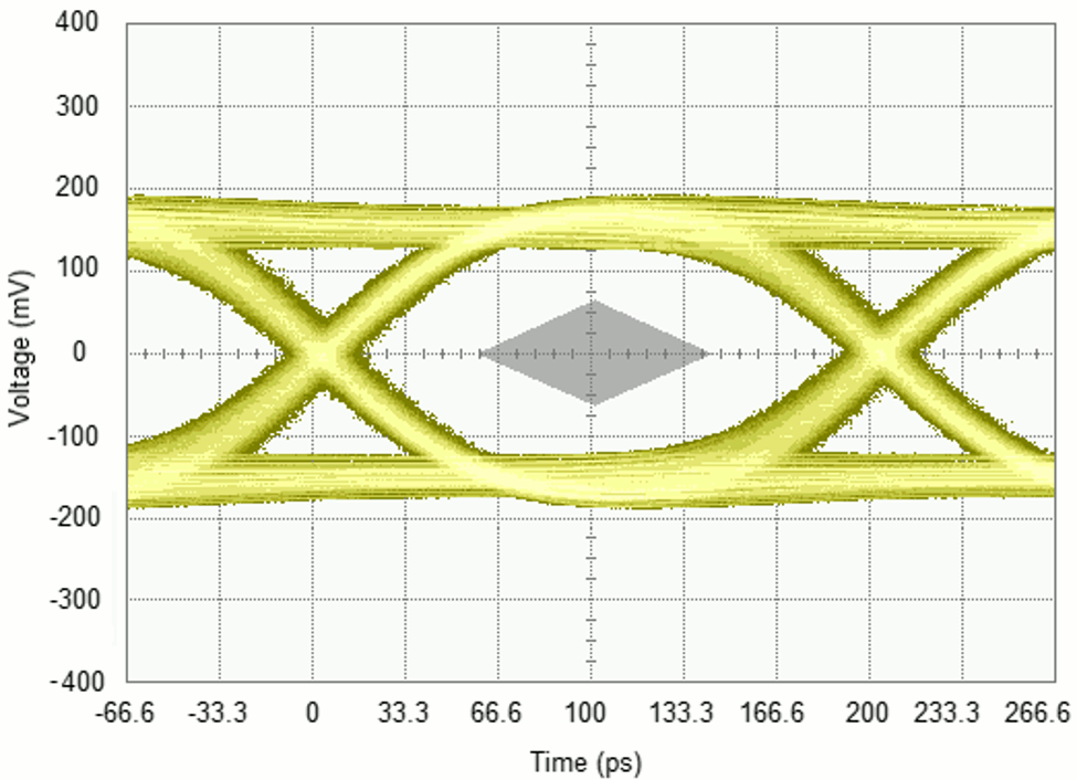
| FSR | Serial bit rate | 1.0 | 5.0 | Gb/s | ||
| UI | Unit Interval 5.0 Gb/s Data Rate |
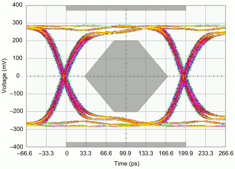
200 | ps | |||
| tR, tF | Edge transition rise and fall times | 40 | ps | |||
| DJ | Deterministic jitter Includes periodic jitter (PJ), data dependent jitter (DDJ), duty cycle distortion (DCD), and inter-symbol interference (ISI); 5.0 Gb/s data rate. |
0.032 | p-p UI | |||
| 6.33 | p-p ps | |||||
| RJ | Random jitter Assumes BER of 1e-15 (Q = 15.88); 5.0 Gb/s data rate |
0.118 | p-p UI | |||
| 1.48 | rms ps | |||||
| TJ | Total jitter Sum of DJ and RJ. Assumes BER of 1e-15 (measured Q = 15.6); 5.0 Gb/s data rate. |
0.148 | p-p UI | |||
| 29.56 | p-p ps | |||||
| SPI BUS TIMING CHARACTERISTICS(1) | ||||||
| fSCLK | Serial clock frequency fSCLK = 1 / tP |
20 | MHz | |||
| tPH | SCLK pulse width – high | 10 | ns | |||
| tPL | SCLK pulse width – low | 10 | ns | |||
| tSSU | SDI input data setup time | 5 | ns | |||
| tSH | SDI input data hold time | 5 | ns | |||
| tODZ | SDO output data driven-to-3-state time | 15 | ns | |||
| tOZD | SDO output data 3-state-to-driven time | 15 | ns | |||
| tOD | SDO output data delay time | 20 | ns | |||
| tCSS | CSB setup time | 5 | ns | |||
| tCSH | CSB hold time | 5 | ns | |||
| tIAG | Inter-access gap Minimum time CSB must be de-asserted between accesses |
5 | ns | |||
(1) All timing specifications for the SPI given for VSPI = 1.8-V logic levels and a 5-pF capacitive load on the SDO output. Timing specification may require larger margins for VSPI= 1.2 V.
(2) This parameter is verified by design.
 Figure 1. Electrical Level Diagram for Differential Input Signals
 Figure 2. Simplified Electrical Circuit Diagram for Differential Input Signals
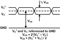 Figure 3. Electrical Level Diagram for Differential Output Signals
 Figure 4. Electrical Circuit Diagram for Differential Output Signals
 Figure 5. Electrical Level Diagram for Single-ended Digital Inputs and Outputs
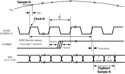 Figure 6. Sample to Data Timing Diagram
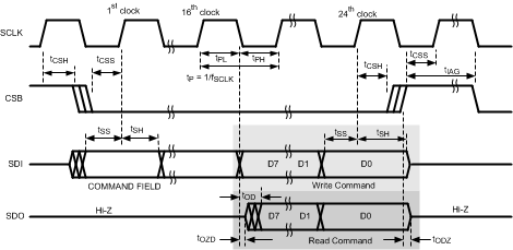 Figure 7. SPI Timing Diagram
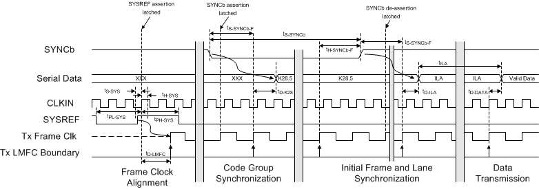 Figure 8. JESD204B Interface Link Initialization Timing Diagram
For more information, see the Functional Block Diagram.
6.13 Typical Characteristics
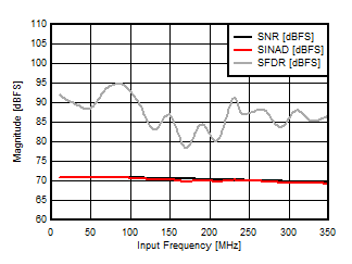
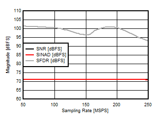
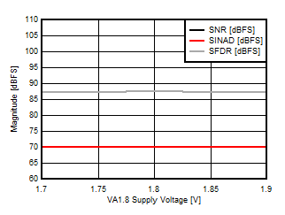
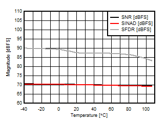
Unless otherwise noted, these specifications apply for VA3.0 = 3.0 V; VA1.8 = 1.8 V; VA1.2 = 1.2 V; FCLKIN = FS = 250 MSPS; 240-MHz input frequency; –3-dBFS input power. External termination at ADC input is 66 Ω differential. CLKIN± input is a 2 Vp-p differential sinusoid. Typical values are at TA = 25°C.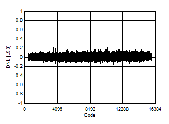
| Input Frequency | = 10 MHz | |
| Input Frequency | = 10 MHz | |
| Input Frequency | = 10 MHz |
| Nominal Supplies: | VA3.0 = 3.0 V | VA1.2 = 1.2 V |
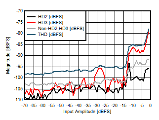
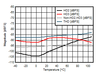
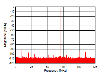
| SNR = 70.9 dBFS | Capture Depth = | 65536 Samples |
| SFDR = 92 dBFS |
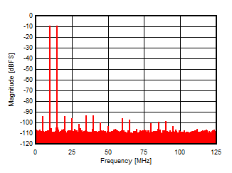
| Input Amplitude = | IMD3 = –94 dBFS | Capture Depth = |
| –9 dBFS/tone | 65536 Samples |
| Input Frequency | = 10 MHz | |
| Input Frequency | = 10 MHz | |
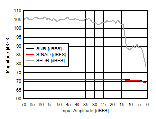
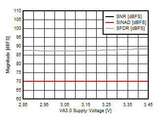
| Nominal Supplies: | VA1.8 = 1.8 V | VA1.2 = 1.2 V |
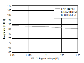
| Nominal Supplies: | VA3.0 = 3.0 V | VA1.8 = 1.8 V |
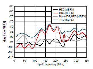
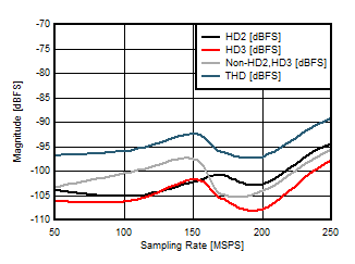
| Input Frequency | = 10 MHz |
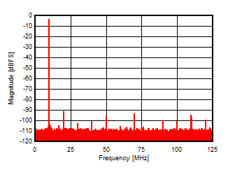
| SNR = 71.0 dBFS | Capture Depth = | 65536 Samples |
| SFDR = 92 dBFS |
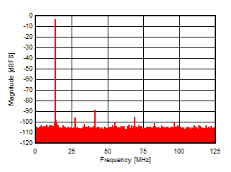
| SNR = 70.1 dBFS | Capture Depth = | 65536 Samples |
| SFDR = 86 dBFS |
