JAJSGV3B September 2015 – January 2019 ADC31JB68
PRODUCTION DATA.
- 1 特長
- 2 アプリケーション
- 3 概要
- 4 改訂履歴
- 5 概要(続き)
- 6 Pin Configuration and Functions
- 7 Specifications
- 8 Parameter Measurement Information
-
9 Detailed Description
- 9.1 Overview
- 9.2 Functional Block Diagram
- 9.3
Feature Description
- 9.3.1 Analog Inputs and Input Buffer
- 9.3.2 Amplitude and Phase Imbalance Correction
- 9.3.3 Over-Range Detection
- 9.3.4 Input Clock Divider
- 9.3.5 SYSREF Detection Gate
- 9.3.6 Serial Differential Output Drivers
- 9.3.7 ADC Core Calibration
- 9.3.8 Data Format
- 9.3.9 JESD204B Supported Features
- 9.3.10 JESD204B Interface
- 9.3.11 Transport Layer Configuration
- 9.3.12 Test Pattern Sequences
- 9.3.13 JESD204B Link Initialization
- 9.3.14 SPI
- 9.4 Device Functional Modes
- 9.5
Register Map
- 9.5.1
Register Descriptions
- 9.5.1.1 CONFIG_A (address = 0x0000) [reset = 0x3C]
- 9.5.1.2 DEVICE CONFIG (address = 0x0002) [reset = 0x00]
- 9.5.1.3 CHIP_TYPE (address = 0x0003 ) [reset = 0x03]
- 9.5.1.4 CHIP_ID (address = 0x0005, 0x0004) [reset = 0x00, 0x1B]
- 9.5.1.5 CHIP_VERSION (address =0x0006) [reset = 0x00]
- 9.5.1.6 VENDOR_ID (address = 0x000D, 0x000C) [reset = 0x04, 0x51]
- 9.5.1.7 SPI_CFG (address = 0x0010 ) [reset = 0x01]
- 9.5.1.8 OM1 (Operational Mode 1) (address = 0x0012) [reset = 0xC1]
- 9.5.1.9 OM2 (Operational Mode 2) (address = 0x0013) [reset = 0x20]
- 9.5.1.10 IMB_ADJ (Imbalance Adjust) (address = 0x0014) [reset = 0x00]
- 9.5.1.11 OVR_EN (Over-Range Enable) (address = 0x003A) [reset = 0x00]
- 9.5.1.12 OVR_HOLD (Over-Range Hold) (address = 0x003B) [reset = 0x00]
- 9.5.1.13 OVR_TH (Over-Range Threshold) (address = 0x003C) [reset = 0x00]
- 9.5.1.14 DC_MODE (DC Offset Correction Mode) (address = 0x003D) [reset = 0x00]
- 9.5.1.15 SER_CFG (Serial Lane Transmitter Configuration) (address = 0x0047) [reset = 0x00]
- 9.5.1.16 JESD_CTRL1 (JESD Configuration Control 1) (address = 0x0060) [reset = 0x7F]
- 9.5.1.17 JESD_CTRL2 (JESD Configuration Control 2) (address = 0x0061) [reset = 0x00]
- 9.5.1.18 JESD_RSTEP (JESD Ramp Pattern Step) (address = 0x0063, 0x0062) [reset = 0x00, 0x01]
- 9.5.1.19 SER_INV (Serial Lane Inversion Control) (address = 0x0064) [reset = 0x00]
- 9.5.1.20 JESD_STATUS (JESD Link Status) (address = 0x006C) [reset = N/A]
- 9.5.1
Register Descriptions
- 10Application and Implementation
- 11Power Supply Recommendations
- 12Layout
- 13デバイスおよびドキュメントのサポート
- 14メカニカル、パッケージ、および注文情報
パッケージ・オプション
メカニカル・データ(パッケージ|ピン)
- RTA|40
サーマルパッド・メカニカル・データ
- RTA|40
発注情報
9.3.14 SPI
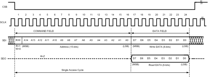
The SPI allows access to the internal configuration registers of the ADC through read and write commands to a specific address. The interface protocol has a 1-bit command, 15-bit address word and 8-bit data word as shown in Figure 37. A read or write command is 24 bits in total, starting with the read or write command bit where 0 indicates a write command and 1 indicates a read command. The read or write command bit is clocked into the device on the first rising edge of SCLK after CSb is asserted to 0. During a write command, the 15-bit address and 8-bit data values follow the read or write bit MSB-first and are latched on the rising edge of SCLK. During a read command, the SDO output is enabled shortly after the 16th rising edge of SCLK and outputs the read value MSB first before the SDO output is returned to a high impedance state. The read or write command is completed on the SCLK rising edge on which the data word’s LSB is latched. CSb may be de-asserted to 1 after the LSB is latched into the device.
The SPI allows command streaming where multiple commands are made without de-asserting CSb in-between commands. The commands in the stream must be of similar types, either read or write. Each subsequent command applies to the register address adjacent to the register accessed in the previous command. The address order can be configured as either ascending or descending. Command streaming is accomplished by immediately following a completed command with another set of 8 rising edges of SCLK without de-asserting CSb. During a write command, an 8-bit data word is input on the SDI input for each subsequent set of SCLK edges. During a read command, data is output from SDO for each subsequent set of SCLK edges. Each subsequent command is considered finished after the 8th rising edge of SCLK. De-asserting CSb aborts an incomplete command.
The SDO output is high impedance at all times other than during the final portion of a read command. During the time that the SDO output is active, the logic level is determined by a configuration register. The SPI output logic level must be properly configured after power up and before making a read command to prevent damaging the receiving device or any other device connected to the SPI bus. Until the SPI_CFG register is properly configured, voltages on the SDO output may be as high as the VA3.0 supply during a read command. The SDI, SCLK, and CSB pins are all 1.2-V to 3.0-V compatible.
 Figure 37. Serial Interface Protocol