JAJSGV3B September 2015 – January 2019 ADC31JB68
PRODUCTION DATA.
- 1 特長
- 2 アプリケーション
- 3 概要
- 4 改訂履歴
- 5 概要(続き)
- 6 Pin Configuration and Functions
- 7 Specifications
- 8 Parameter Measurement Information
-
9 Detailed Description
- 9.1 Overview
- 9.2 Functional Block Diagram
- 9.3
Feature Description
- 9.3.1 Analog Inputs and Input Buffer
- 9.3.2 Amplitude and Phase Imbalance Correction
- 9.3.3 Over-Range Detection
- 9.3.4 Input Clock Divider
- 9.3.5 SYSREF Detection Gate
- 9.3.6 Serial Differential Output Drivers
- 9.3.7 ADC Core Calibration
- 9.3.8 Data Format
- 9.3.9 JESD204B Supported Features
- 9.3.10 JESD204B Interface
- 9.3.11 Transport Layer Configuration
- 9.3.12 Test Pattern Sequences
- 9.3.13 JESD204B Link Initialization
- 9.3.14 SPI
- 9.4 Device Functional Modes
- 9.5
Register Map
- 9.5.1
Register Descriptions
- 9.5.1.1 CONFIG_A (address = 0x0000) [reset = 0x3C]
- 9.5.1.2 DEVICE CONFIG (address = 0x0002) [reset = 0x00]
- 9.5.1.3 CHIP_TYPE (address = 0x0003 ) [reset = 0x03]
- 9.5.1.4 CHIP_ID (address = 0x0005, 0x0004) [reset = 0x00, 0x1B]
- 9.5.1.5 CHIP_VERSION (address =0x0006) [reset = 0x00]
- 9.5.1.6 VENDOR_ID (address = 0x000D, 0x000C) [reset = 0x04, 0x51]
- 9.5.1.7 SPI_CFG (address = 0x0010 ) [reset = 0x01]
- 9.5.1.8 OM1 (Operational Mode 1) (address = 0x0012) [reset = 0xC1]
- 9.5.1.9 OM2 (Operational Mode 2) (address = 0x0013) [reset = 0x20]
- 9.5.1.10 IMB_ADJ (Imbalance Adjust) (address = 0x0014) [reset = 0x00]
- 9.5.1.11 OVR_EN (Over-Range Enable) (address = 0x003A) [reset = 0x00]
- 9.5.1.12 OVR_HOLD (Over-Range Hold) (address = 0x003B) [reset = 0x00]
- 9.5.1.13 OVR_TH (Over-Range Threshold) (address = 0x003C) [reset = 0x00]
- 9.5.1.14 DC_MODE (DC Offset Correction Mode) (address = 0x003D) [reset = 0x00]
- 9.5.1.15 SER_CFG (Serial Lane Transmitter Configuration) (address = 0x0047) [reset = 0x00]
- 9.5.1.16 JESD_CTRL1 (JESD Configuration Control 1) (address = 0x0060) [reset = 0x7F]
- 9.5.1.17 JESD_CTRL2 (JESD Configuration Control 2) (address = 0x0061) [reset = 0x00]
- 9.5.1.18 JESD_RSTEP (JESD Ramp Pattern Step) (address = 0x0063, 0x0062) [reset = 0x00, 0x01]
- 9.5.1.19 SER_INV (Serial Lane Inversion Control) (address = 0x0064) [reset = 0x00]
- 9.5.1.20 JESD_STATUS (JESD Link Status) (address = 0x006C) [reset = N/A]
- 9.5.1
Register Descriptions
- 10Application and Implementation
- 11Power Supply Recommendations
- 12Layout
- 13デバイスおよびドキュメントのサポート
- 14メカニカル、パッケージ、および注文情報
パッケージ・オプション
メカニカル・データ(パッケージ|ピン)
- RTA|40
サーマルパッド・メカニカル・データ
- RTA|40
発注情報
10.1.1.1 Internal Noise Sources
The signal to noise ratio of the ADC is limited by the following noise sources inherent to the device: 1) Quantization Noise, 2) Thermal Noise, 3) Sampling Instant Noise (Aperture Jitter). These sources combine together to limit the noise performance of the converter as described by Equation 1. Noise sources external to the ADC can generally be included in this equation as an RMS summation to determine system performance.

Quantization noise is independent of the input signal but does not affect the noise performance of the ADC31JB68 because the SNR limitation of a 16-bit ADC due to quantization noise is 96-dB, well above the SNR of this device. The thermal noise is input independent, spread evenly across the spectrum, and the main limitation for signals with lower frequencies or lower amplitudes.
If quantization and thermal noise is ignored, the fundamental SNR limitation due to aperture jitter can be calculated using Equation 2.
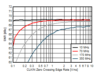
Signals with larger amplitudes and higher frequencies introduce signal dependent sampling instant noise due to the Jitter on the sampling clock edge. This noise includes a broadband component that raises the overall noise spectral density as well as a in-close noise component that is spectrally shaped and concentrates around the signal in the spectrum. The differential clock receiver of the ADC31JB68 has a very-low noise floor and wide bandwidth. Minimizing the aperture jitter requires a sampling clock with a steep edge rate at the zero crossing. Lesser edge rates increase the aperture jitter as demonstrated in Figure 58 which shows the SNR limitation due to aperture jitter as a function of clock edge range and input signal frequency.
 Figure 58. Aperture Jitter vs Input Clock Edge Rate, -1 dBFS Input Signal