SBAS663A May 2014 – June 2015 ADC32J42 , ADC32J43 , ADC32J44 , ADC32J45
PRODUCTION DATA.
- 1 Features
- 2 Applications
- 3 Description
- 4 Revision History
- 5 Device Comparison Table
- 6 Pin Configuration and Functions
-
7 Specifications
- 7.1 Absolute Maximum Ratings
- 7.2 ESD Ratings
- 7.3 Recommended Operating Conditions
- 7.4 Thermal Information
- 7.5 Electrical Characteristics
- 7.6 Electrical Characteristics: ADC32J44, ADC32J45
- 7.7 Electrical Characteristics: ADC32J42, ADC32J43
- 7.8 AC Performance: ADC32J45
- 7.9 AC Performance: ADC32J44
- 7.10 AC Performance: ADC32J43
- 7.11 AC Performance: ADC32J42
- 7.12 Digital Characteristics
- 7.13 Timing Requirements
- 7.14 Typical Characteristics: ADC32J45
- 7.15 Typical Characteristics: ADC32J44
- 7.16 Typical Characteristics: ADC32J43
- 7.17 Typical Characteristics: ADC32J42
- 7.18 Typical Characteristics: Common Plots
- 7.19 Typical Characteristics: Contour Plots
- 8 Parameter Measurement Information
-
9 Detailed Description
- 9.1 Overview
- 9.2 Functional Block Diagram
- 9.3 Feature Description
- 9.4 Device Functional Modes
- 9.5 Programming
- 9.6
Register Maps
- 9.6.1 Summary of Special Mode Registers
- 9.6.2
Serial Register Descriptions
- 9.6.2.1 Register 01h (address = 01h)
- 9.6.2.2 Register 03h (address = 03h)
- 9.6.2.3 Register 04h (address = 04h)
- 9.6.2.4 Register 06h (address = 06h)
- 9.6.2.5 Register 07h (address = 07h)
- 9.6.2.6 Register 08h (address = 08h)
- 9.6.2.7 Register 09h (address = 09h)
- 9.6.2.8 Register 0Ah (address = 0Ah)
- 9.6.2.9 Register 0Bh (address = 0Bh)
- 9.6.2.10 Register 0Ch (address = 0Ch)
- 9.6.2.11 Register 0Dh (address = 0Dh)
- 9.6.2.12 Register 0Eh (address = 0Eh)
- 9.6.2.13 Register 0Fh (address = 0Fh)
- 9.6.2.14 Register 13h (address = 13h)
- 9.6.2.15 Register 15h (address = 15h)
- 9.6.2.16 Register 27h (address = 27h)
- 9.6.2.17 Register 2Ah (address = 2Ah)
- 9.6.2.18 Register 2Bh (address = 2Bh)
- 9.6.2.19 Register 2Fh (address = 2Fh)
- 9.6.2.20 Register 30h (address = 30h)
- 9.6.2.21 Register 31h (address = 31h)
- 9.6.2.22 Register 34h (address = 34h)
- 9.6.2.23 Register 3Ah (address = 3Ah)
- 9.6.2.24 Register 3Bh (address = 3Bh)
- 9.6.2.25 Register 3Ch (address = 3Ch)
- 9.6.2.26 Register 422h (address = 422h)
- 9.6.2.27 Register 434h (address = 434h)
- 9.6.2.28 Register 522h (address = 522h)
- 9.6.2.29 Register 534h (address = 534h)
- 10Application and Implementation
- 11Power-Supply Recommendations
- 12Layout
- 13Device and Documentation Support
- 14Mechanical, Packaging, and Orderable Information
パッケージ・オプション
メカニカル・データ(パッケージ|ピン)
- RGZ|48
サーマルパッド・メカニカル・データ
- RGZ|48
発注情報
8 Parameter Measurement Information
8.1 Timing Diagrams

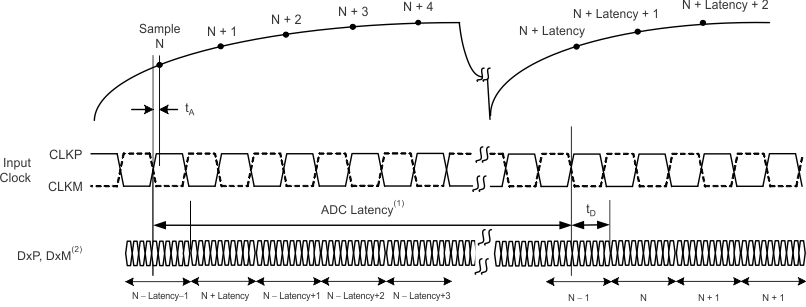
1. Overall latency = ADC latency + tD.
2. x = A for channel A and B for channel B.
Figure 143. ADC Latency

1. x = A for channel A and B for channel B.
Figure 144. SYNC~ Latency in CGS Phase

1. x = A for channel A and B for channel B.
Figure 145. SYNC~ Latency in ILAS Phase
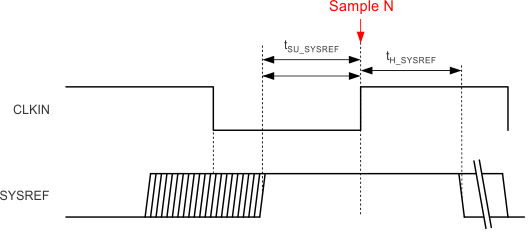
 Figure 146. SYSREF Timing (Subclass 1)
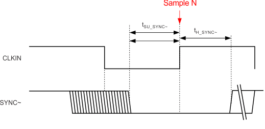
 Figure 147. SYNC~ Timing (Subclass 2)