JAJSOU1B june 2022 – august 2023 ADC32RF54 , ADC32RF55
PRODUCTION DATA
- 1
- 1 特長
- 2 アプリケーション
- 3 概要
- 4 Revision History
- 5 Pin Configuration and Functions
-
6 Specifications
- 6.1 Absolute Maximum Ratings
- 6.2 ESD Ratings
- 6.3 Recommended Operating Conditions
- 6.4 Thermal Information
- 6.5 Electrical Characteristics - Power Consumption
- 6.6 Electrical Characteristics - DC Specifications
- 6.7 Electrical Characteristics - ADC32RF54 AC Specifications (Dither DISABLED)
- 6.8 Electrical Characteristics - ADC32RF54 AC Specifications (Dither ENABLED)
- 6.9 Electrical Characteristics - ADC32RF55 AC Specifications (Dither DISABLED)
- 6.10 Electrical Characteristics - ADC32RF55 AC Specifications (Dither ENABLED)
- 6.11 Timing Requirements
- 6.12 Typical Characteristics - ADC32RF54
- 6.13 Typical Characteristics - ADC32RF55
-
7 Detailed Description
- 7.1 Overview
- 7.2 Functional Block Diagram
- 7.3
Feature Description
- 7.3.1 Analog Inputs
- 7.3.2 Sampling Clock Input
- 7.3.3 SYSREF
- 7.3.4 ADC Foreground Calibration
- 7.3.5 Decimation Filter
- 7.3.6
JESD204B Interface
- 7.3.6.1 JESD204B Initial Lane Alignment (ILA)
- 7.3.6.2 JESD204B Frame Assembly
- 7.3.6.3 JESD204B Frame Assembly in Bypass Mode
- 7.3.6.4 JESD204B Frame Assembly with Complex Decimation - Single Band
- 7.3.6.5 JESD204B Frame Assembly with Real Decimation - Single Band
- 7.3.6.6 JESD204B Frame Assembly with Complex Decimation - Dual Band
- 7.3.6.7 JESD204B Frame Assembly with Complex Decimation - Quad Band
- 7.3.7 SERDES Output MUX
- 7.3.8 Test Pattern
- 7.4 Device Functional Modes
- 7.5 Programming
- 7.6 Register Maps
-
8 Application and Implementation
- 8.1 Application Information
- 8.2 Typical Applications
- 8.3
Initialization Set Up
- 8.3.1
Initial Device Configuration After Power-Up
- 8.3.1.1 STEP 1: RESET
- 8.3.1.2 STEP 2: Device Configuration
- 8.3.1.3 STEP 3: JESD Interface Configuration (1)
- 8.3.1.4 STEP 4: SYSREF Synchronization
- 8.3.1.5 STEP 5: JESD Interface Configuration (2)
- 8.3.1.6 STEP 6: Analog Trim Settings
- 8.3.1.7 STEP 7: Calibration Configuration
- 8.3.1.8 STEP 8: SYSREF Synchronization
- 8.3.1.9 STEP 9: Run Power up Calibration
- 8.3.1.10 STEP 10: JESD Interface Synchronization
- 8.3.1
Initial Device Configuration After Power-Up
- 8.4 Power Supply Recommendations
- 8.5 Layout
- 9 Device and Documentation Support
- 10Mechanical, Packaging, and Orderable Information
7.4.1 Digital Averaging
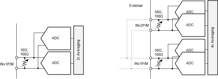
The ADC32RF5x provides a total of eight internal single core 3.0 Gsps ADCs. Normal bypass mode uses only two ADC cores (one ADC per channel). However, the additional six ADCs can be used to trade off further noise density improvement against additional power consumption. Figure 7-45 shows the internal block diagrams for the digital averaging modes. In averaging mode the output resolution is increased to 16-bit to avoid quantization noise limitation.
In 2x averaging mode (left), one external input is connected to the INx1 input where two ADC cores internally average the input signal. In 4x averaging (right), the signal has to be split externally and connected to both the INx1 and INx2 inputs where four ADC cores internally average the signal.
 Figure 7-45 Internal digital averaging (left: 2x, right: 4x)
Table 7-50 provides a trade-off comparison of the 3 different averaging mode options vs the default, non-averaged mode.
| # of ADCs averaged | ADC inputs used for averaging | Input Bandwidth (-3 dB) |
Selected differential input termination | Noise density | Power/ch (W) |
|---|---|---|---|---|---|
| Default | INx1 |
2.75 GHz |
100 Ω | -156 dBFS/Hz | ~2.1 |
| 2 | INx1 |
2.75 GHz |
100 Ω | -158 dBFS/Hz | ~2.6 |
| 4 | INx1, INx2 |
2.1 GHz |
100 Ω | -160 dBFS/Hz | ~3.5 |
Digital averaging improves decorrelated noise contributions by 3 dB per 2x AVG (ideal) while correlated noise does not improve with averaging. Some of the dominant noise sources are correlated, that is, clock jitter (external or first clock input buffer), or power supply noise. While others (such as, ADC thermal noise, clock distribution buffers) are decorrelated. Table 7-51 illustrates a performance example comparison across averaging options.
SNR: When operating close to ADC fullscale, some of the SNR limitation is due to jitter and hence the SNR improvement will not reach 3 dB (2x AVG) or 6 dB (4x AVG). As the input fullscale is reduced, the clock jitter contribution to SNR becomes less and the SNR improvement is approaching the ideal 3 dB per 2x AVG. The same phenomenon can be observed when using digital decimation. As the decimation factor increases, the close-in (correlated noise) becomes the more dominating noise unless the input signal amplitude is reduced.
SFDR: The amplitude of low order harmonics (HD2-HD5) and IMD3 typically is similar across ADCs; thus, the improvement with averaging is small.
| Parameter | Input Amplitude (dBFS) | 1x AVG | 2x AVG | 4x AVG |
|---|---|---|---|---|
| SNR (dBFS) | -4 | 62.8 | 64.9 | 67.2 |
| -10 | 63.9 | 66.3 | 68.2 | |
| -20 | 64.0 | 66.4 | 69.4 | |
| HD2 (dBc) | -4 | 66 | 62 | 71 |
| -10 | 74 | 74 | 75 | |
| -20 | 70 | 70 | 80 | |
| HD3 (dBc) | -4 | 73 | 76 | 78 |
| -10 | 80 | 78 | 80 | |
| -20 | 74 | 71 | 72 | |
| Non HD23 (dBFS) | -4 | 86 | 84 | 83 |
| -10 | 90 | 91 | 92 | |
| -20 | 96 | 100 | 97 | |
| IMD3 (dBc) | -10 dBFS/tone | 77 | 73 | 71 |
| -20 dBFS/tone | 78 | 79 | 72 |