JAJSCV8B May 2016 – December 2021 ADC32RF80 , ADC32RF83
PRODUCTION DATA
- 1 特長
- 2 アプリケーション
- 3 説明
- 4 Revision History
- 5 Pin Configuration and Functions
-
6 Specifications
- 6.1 Absolute Maximum Ratings
- 6.2 ESD Ratings
- 6.3 Recommended Operating Conditions
- 6.4 Thermal Information
- 6.5 Electrical Characteristics
- 6.6 AC Performance Characteristics: fS = 2949.12 MSPS
- 6.7 AC Performance Characteristics: fS = 2457.6 MSPS (Performance Optimized for F + A + D Band)
- 6.8 AC Performance Characteristics: fS = 2457.6 MSPS (Performance Optimized for F + A Band)
- 6.9 Digital Requirements
- 6.10 Timing Requirements
- 6.11 Typical Characteristics
- 7 Parameter Measurement Information
-
8 Detailed Description
- 8.1 Overview
- 8.2 Functional Block Diagram
- 8.3
Feature Description
- 8.3.1 Analog Inputs
- 8.3.2 Clock Input
- 8.3.3 SYSREF Input
- 8.3.4 DDC Block
- 8.3.5 NCO Switching
- 8.3.6 SerDes Transmitter Interface
- 8.3.7 Eye Diagrams
- 8.3.8 Alarm Outputs: Power Detectors for AGC Support
- 8.3.9 Power-Down Mode
- 8.3.10 ADC Test Pattern
- 8.4
Device Functional Modes
- 8.4.1 Device Configuration
- 8.4.2
JESD204B Interface
- 8.4.2.1 JESD204B Initial Lane Alignment (ILA)
- 8.4.2.2 JESD204B Frame Assembly
- 8.4.2.3 JESD204B Frame Assembly with Decimation (Single-Band DDC): Complex Output
- 8.4.2.4 JESD204B Frame Assembly with Decimation (Single-Band DDC): Real Output
- 8.4.2.5 JESD204B Frame Assembly with Decimation (Single-Band DDC): Real Output
- 8.4.2.6 JESD204B Frame Assembly with Decimation (Dual-Band DDC): Complex Output
- 8.4.2.7 JESD204B Frame Assembly with Decimation (Dual-Band DDC): Real Output
- 8.4.3 Serial Interface
- 8.5
Register Maps
- 8.5.1 Example Register Writes
- 8.5.2
Register Descriptions
- 8.5.2.1
General Registers
- 8.5.2.1.1 Register 000h (address = 000h), General Registers
- 8.5.2.1.2 Register 002h (address = 002h), General Registers
- 8.5.2.1.3 Register 003h (address = 003h), General Registers
- 8.5.2.1.4 Register 004h (address = 004h), General Registers
- 8.5.2.1.5 Register 010h (address = 010h), General Registers
- 8.5.2.1.6 Register 011h (address = 011h), General Registers
- 8.5.2.1.7 Register 012h (address = 012h), General Registers
- 8.5.2.1
General Registers
- 8.5.3
Master Page (M = 0)
- 8.5.3.1 Register 020h (address = 020h), Master Page
- 8.5.3.2 Register 032h (address = 032h), Master Page
- 8.5.3.3 Register 039h (address = 039h), Master Page
- 8.5.3.4 Register 03Ch (address = 03Ch), Master Page
- 8.5.3.5 Register 05Ah (address = 05Ah), Master Page
- 8.5.3.6 Register 03Dh (address = 3Dh), Master Page
- 8.5.3.7 Register 057h (address = 057h), Master Page
- 8.5.3.8 Register 058h (address = 058h), Master Page
- 8.5.4 ADC Page (FFh, M = 0)
- 8.5.5 Digital Function Page (610000h, M = 1 for Channel A and 610100h, M = 1 for Channel B)
- 8.5.6 Offset Corr Page Channel A (610000h, M = 1)
- 8.5.7 Offset Corr Page Channel B (610000h, M = 1)
- 8.5.8 Digital Gain Page (610005h, M = 1 for Channel A and 610105h, M = 1 for Channel B)
- 8.5.9 Main Digital Page Channel A (680000h, M = 1)
- 8.5.10 Main Digital Page Channel B (680001h, M = 1)
- 8.5.11
JESD Digital Page (6900h, M = 1)
- 8.5.11.1 Register 001h (address = 001h), JESD Digital Page
- 8.5.11.2 Register 002h (address = 002h ), JESD Digital Page
- 8.5.11.3 Register 003h (address = 003h), JESD Digital Page
- 8.5.11.4 Register 004h (address = 004h), JESD Digital Page
- 8.5.11.5 Register 006h (address = 006h), JESD Digital Page
- 8.5.11.6 Register 007h (address = 007h), JESD Digital Page
- 8.5.11.7 Register 016h (address = 016h), JESD Digital Page
- 8.5.11.8 Register 017h (address = 017h), JESD Digital Page
- 8.5.11.9 Register 032h-035h (address = 032h-035h), JESD Digital Page
- 8.5.11.10 Register 036h (address = 036h), JESD Digital Page
- 8.5.11.11 Register 037h (address = 037h), JESD Digital Page
- 8.5.11.12 Register 03Ch (address = 03Ch), JESD Digital Page
- 8.5.11.13 Register 03Eh (address = 03Eh), JESD Digital Page
- 8.5.12
Decimation Filter Page
- 8.5.12.1 Register 000h (address = 000h), Decimation Filter Page
- 8.5.12.2 Register 001h (address = 001h), Decimation Filter Page
- 8.5.12.3 Register 002h (address = 2h), Decimation Filter Page
- 8.5.12.4 Register 005h (address = 005h), Decimation Filter Page
- 8.5.12.5 Register 006h (address = 006h), Decimation Filter Page
- 8.5.12.6 Register 007h (address = 007h), Decimation Filter Page
- 8.5.12.7 Register 008h (address = 008h), Decimation Filter Page
- 8.5.12.8 Register 009h (address = 009h), Decimation Filter Page
- 8.5.12.9 Register 00Ah (address = 00Ah), Decimation Filter Page
- 8.5.12.10 Register 00Bh (address = 00Bh), Decimation Filter Page
- 8.5.12.11 Register 00Ch (address = 00Ch), Decimation Filter Page
- 8.5.12.12 Register 00Dh (address = 00Dh), Decimation Filter Page
- 8.5.12.13 Register 00Eh (address = 00Eh), Decimation Filter Page
- 8.5.12.14 Register 00Fh (address = 00Fh), Decimation Filter Page
- 8.5.12.15 Register 010h (address = 010h), Decimation Filter Page
- 8.5.12.16 Register 011h (address = 011h), Decimation Filter Page
- 8.5.12.17 Register 014h (address = 014h), Decimation Filter Page
- 8.5.12.18 Register 016h (address = 016h), Decimation Filter Page
- 8.5.12.19 Register 01Eh (address = 01Eh), Decimation Filter Page
- 8.5.12.20 Register 01Fh (address = 01Fh), Decimation Filter Page
- 8.5.12.21 Register 033h-036h (address = 033h-036h), Decimation Filter Page
- 8.5.12.22 Register 037h (address = 037h), Decimation Filter Page
- 8.5.12.23 Register 03Ah (address = 03Ah), Decimation Filter Page
- 8.5.13
Power Detector Page
- 8.5.13.1 Register 000h (address = 000h), Power Detector Page
- 8.5.13.2 Register 001h-002h (address = 001h-002h), Power Detector Page
- 8.5.13.3 Register 003h (address = 003h), Power Detector Page
- 8.5.13.4 Register 007h-00Ah (address = 007h-00Ah), Power Detector Page
- 8.5.13.5 Register 00Bh-00Ch (address = 00Bh-00Ch), Power Detector Page
- 8.5.13.6 Register 00Dh (address = 00Dh), Power Detector Page
- 8.5.13.7 Register 00Eh (address = 00Eh), Power Detector Page
- 8.5.13.8 Register 00Fh, 010h-012h, and 016h-019h (address = 00Fh, 010h-012h, and 016h-019h), Power Detector Page
- 8.5.13.9 Register 013h-01Ah (address = 013h-01Ah), Power Detector Page
- 8.5.13.10 Register 01Dh-01Eh (address = 01Dh-01Eh), Power Detector Page
- 8.5.13.11 Register 020h (address = 020h), Power Detector Page
- 8.5.13.12 Register 021h (address = 021h), Power Detector Page
- 8.5.13.13 Register 022h-025h (address = 022h-025h), Power Detector Page
- 8.5.13.14 Register 027h (address = 027h), Power Detector Page
- 8.5.13.15 Register 02Bh (address = 02Bh), Power Detector Page
- 8.5.13.16 Register 032h-035h (address = 032h-035h), Power Detector Page
- 8.5.13.17 Register 037h (address = 037h), Power Detector Page
- 8.5.13.18 Register 038h (address = 038h), Power Detector Page
- 9 Application and Implementation
- 10Power Supply Recommendations
- 11Layout
- 12Device and Documentation Support
- 13Mechanical, Packaging, and Orderable Information
パッケージ・オプション
メカニカル・データ(パッケージ|ピン)
サーマルパッド・メカニカル・データ
発注情報
8.4.3 Serial Interface
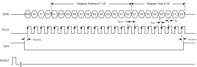
The ADC has a set of internal registers that can be accessed by the serial interface formed by the SEN (serial interface enable), SCLK (serial interface clock), and SDIN (serial interface data) pins. Serially shifting bits into the device is enabled when SEN is low. SDIN serial data are latched at every SCLK rising edge when SEN is active (low), as shown in Figure 8-56. The interface can function with SCLK frequencies from 20 MHz down to low speeds (of a few hertz) and also with a non-50% SCLK duty cycle, as shown in Table 8-25.
The SPI access uses 24 bits consisting of eight register data bits, 12 register address bits, and four special bits to distinguish between read/write, page and register, and individual channel access, as described in Table 8-26.
 Figure 8-56 SPI Timing Diagram
| MIN | TYP | MAX | UNIT | ||
|---|---|---|---|---|---|
| fSCLK | SCLK frequency (equal to 1 / tSCLK) | 1 | 20 | MHz | |
| tSLOADS | SEN to SCLK setup time | 50 | ns | ||
| tSLOADH | SCLK to SEN hold time | 50 | ns | ||
| tDSU | SDIN setup time | 10 | ns | ||
| tDH | SDIN hold time | 10 | ns | ||
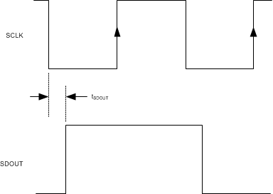
| tSDOUT | Delay between SCLK falling edge to SDOUT | 10 | ns | ||
| SPI BIT | DESCRIPTION | OPTIONS |
|---|---|---|
| R/W bit | Read/write bit | 0 = SPI write 1 = SPI read back |
| M bit | SPI bank access | 0 = Analog SPI bank (master) 1 = All digital SPI banks (main digital, interleaving, decimation filter, JESD digital, and so forth) |
| P bit | JESD page selection bit | 0 = Page access 1 = Register access |
| CH bit | SPI access for a specific channel of the JESD SPI bank | 0 = Channel A 1 = Channel B |
| ADDR[11:0] | SPI address bits | — |
| DATA[7:0] | SPI data bits | — |
Figure 8-57 shows the SDOUT timing when data are read back from a register. Data are placed on the SDOUT bus at the SCLK falling edge so that the data can be latched at the SCLK rising edge by the external receiver.
 Figure 8-57 SDOUT Timing