SBAS669A May 2014 – January 2015 ADC34J22 , ADC34J23 , ADC34J24 , ADC34J25
PRODUCTION DATA.
- 1 Features
- 2 Applications
- 3 Description
- 4 Revision History
- 5 Device Comparison Table
- 6 Pin Configuration and Functions
-
7 Specifications
- 7.1 Absolute Maximum Ratings
- 7.2 ESD Ratings
- 7.3 Recommended Operating Conditions
- 7.4 Summary of Special Mode Registers
- 7.5 Thermal Information
- 7.6 Electrical Characteristics: ADC34J24, ADC34J25
- 7.7 Electrical Characteristics: ADC34J22, ADC34J23
- 7.8 Electrical Characteristics: General
- 7.9 AC Performance: ADC34J25
- 7.10 AC Performance: ADC34J24
- 7.11 AC Performance: ADC34J23
- 7.12 AC Performance: ADC34J22
- 7.13 Digital Characteristics
- 7.14 Timing Characteristics
- 7.15 Typical Characteristics: ADC34J25
- 7.16 Typical Characteristics: ADC34J24
- 7.17 Typical Characteristics: ADC34J23
- 7.18 Typical Characteristics: ADC34J22
- 7.19 Typical Characteristics: Common Plots
- 7.20 Typical Characteristics: Contour Plots
- 8 Parameter Measurement Information
- 9 Detailed Description
- 10Application and Implementation
- 11Power-Supply Recommendations
- 12Layout
- 13Device and Documentation Support
- 14Mechanical, Packaging, and Orderable Information
パッケージ・オプション
メカニカル・データ(パッケージ|ピン)
- RGZ|48
サーマルパッド・メカニカル・データ
- RGZ|48
発注情報
10 Application and Implementation
10.1 Application Information
Typical applications involving transformer-coupled circuits are discussed in this section. Transformers (such as ADT1-1WT or WBC1-1) can be used up to 250 MHz to achieve good phase and amplitude balances at ADC inputs. While designing the dc driving circuits, the ADC input impedance must be considered. Figure 200 and Figure 201 show the impedance (Zin = Rin || Cin) across the ADC input pins.
 Figure 200. Differential Input Resistance, RIN
 Figure 201. Differential Input Capacitance, CIN
10.2 Typical Applications
10.2.1 Driving Circuit Design: Low Input Frequencies
 Figure 202. Driving Circuit for Low Input Frequencies
10.2.1.1 Design Requirements
For optimum performance, the analog inputs must be driven differentially. An optional 5-Ω to 15-Ω resistor in series with each input pin can be kept to damp out ringing caused by package parasitics. The drive circuit may have to be designed to minimize the impact of kick-back noise generated by sampling switches opening and closing inside the ADC, as well as ensuring low insertion loss over the desired frequency range and matched impedance to the source.
10.2.1.2 Detailed Design Procedure
A typical application using two back-to-back coupled transformers is illustrated in Figure 202. The circuit is optimized for low input frequencies. An external R-C-R filter using 50-Ω resistors and a 22-pF capacitor is used. With the series inductor (39 nH), this combination helps absorb the sampling glitches.
10.2.1.3 Application Curve
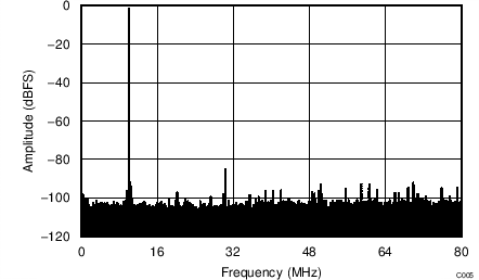
Figure 203 shows the performance obtained by using the circuit shown in Figure 202.

| fS = 160 MSPS | SNR = 70.3 dBFS | |||
| fIN = 10 MHz | SFDR = 84 dBc |
10.2.2 Driving Circuit Design: Input Frequencies Between 100 MHz to 230 MHz
 Figure 204. Driving Circuit for Mid-Range Input Frequencies (100 MHz < fIN < 230 MHz)
10.2.2.1 Design Requirements
See the Design Requirements section for further details.
10.2.2.2 Detailed Design Procedure
When input frequencies are between 100 MHz to 230 MHz, an R-LC-R circuit can be used to optimize performance, as shown in Figure 204.
10.2.2.3 Application Curve
Figure 205 shows the performance obtained by using the circuit shown in Figure 204.

| fS = 160 MSPS | SNR = 67.9 dBFS | |||
| fIN = 170 MHz | SFDR = 84.1 dBc |
10.2.3 Driving Circuit Design: Input Frequencies Greater than 230 MHz
 Figure 206. Driving Circuit for High Input Frequencies (fIN > 230 MHz)
10.2.3.1 Design Requirements
See the Design Requirements section for further details.
10.2.3.2 Detailed Design Procedure
For high input frequencies (> 230 MHz), using the R-C-R or R-LC-R circuit does not show significant improvement in performance. However, a series resistance of 10 Ω can be used as shown in Figure 206.
10.2.3.3 Application Curve
Figure 207 shows the performance obtained by using the circuit shown in Figure 206.

| fS = 160 MSPS | SNR = 63.1 dBFS | |||
| fIN = 450 MHz | SFDR = 73 dBc |