JAJSNQ4 March 2023 ADC34RF52
PRODUCTION DATA
- 1 特長
- 2 アプリケーション
- 3 概要
- 4 Revision History
- 5 Pin Configuration and Functions
-
6 Specifications
- 6.1 Absolute Maximum Ratings
- 6.2 ESD Ratings
- 6.3 Recommended Operating Conditions
- 6.4 Thermal Information
- 6.5 Electrical Characteristics - Power Consumption
- 6.6 Electrical Characteristics - DC Specifications
- 6.7 Electrical Characteristics - AC Specifications (Dither DISABLED)
- 6.8 Electrical Characteristics - AC Specifications (Dither ENABLED)
- 6.9 Timing Requirements
- 6.10 Typical Characteristics
-
7 Detailed Description
- 7.1 Overview
- 7.2 Functional Block Diagram
- 7.3
Feature Description
- 7.3.1 Analog Inputs
- 7.3.2 Sampling Clock Input
- 7.3.3 SYSREF
- 7.3.4 ADC Foreground Calibration
- 7.3.5 Decimation Filter
- 7.3.6 JESD204B Interface
- 7.3.7 Test Pattern
- 7.4 Device Functional Modes
- 7.5 Programming
- 7.6 Register Maps
-
8 Application Information Disclaimer
- 8.1 Application Information
- 8.2 Typical Application
- 8.3
Initialization Set Up
- 8.3.1
Initial Device Configuration After Power-Up
- 8.3.1.1 STEP 1: RESET
- 8.3.1.2 STEP 2: Device Configuration
- 8.3.1.3 STEP 3: JESD Interface Configuration (1)
- 8.3.1.4 STEP 4: SYSREF Synchronization
- 8.3.1.5 STEP 5: JESD Interface Configuration (2)
- 8.3.1.6 STEP 6: Analog Trim Settings
- 8.3.1.7 STEP 7: Calibration Configuration
- 8.3.1.8 STEP 8: SYSREF Synchronization
- 8.3.1.9 STEP 9: Run Power up Calibration
- 8.3.1.10 Step 10: JESD Interface Synchronization
- 8.3.1
Initial Device Configuration After Power-Up
- 8.4 Power Supply Recommendations
- 8.5 Layout
- 9 Device and Documentation Support
- 10Mechanical, Packaging, and Orderable Information
7.3.5.1 Decimation Filter Response
This section provides the different decimation filter responses with a normalized ADC sampling rate. The complex filter pass band is ~ 80% (-1 dB) with a minimum of 85 dB stop band rejection.
 Figure 7-21 Complex Decimation by 4
Filter Response
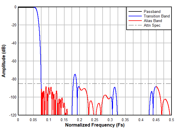 Figure 7-23 Complex Decimation by 8 Filter Response
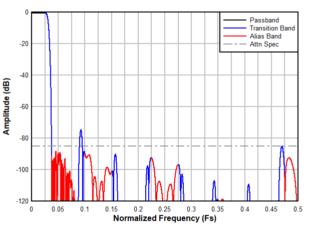 Figure 7-25 Complex Decimation by 16 Filter Response
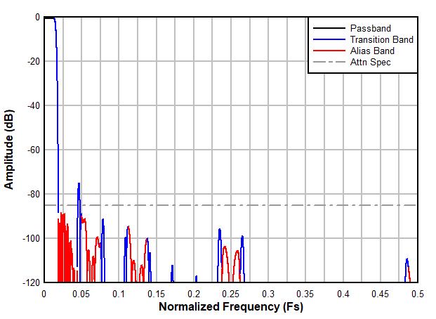 Figure 7-27 Complex Decimation by 32 Filter Response
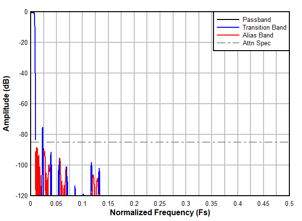 Figure 7-29 Complex Decimation by 64 Filter Response
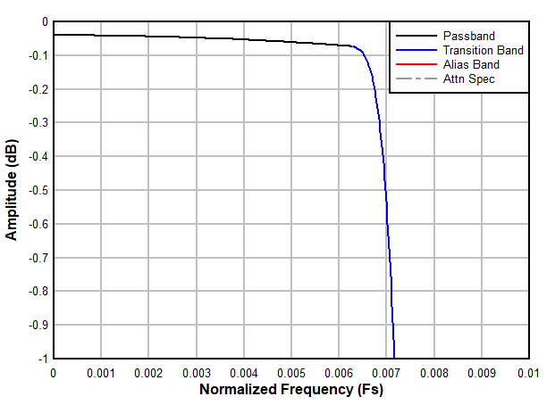 Figure 7-31 Decimation by 64 Passband Ripple Response
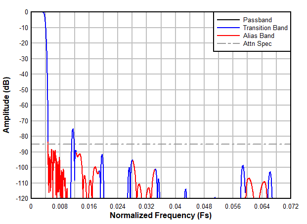 Figure 7-33 Complex Decimation by 128 Filter Response
 Figure 7-22 Decimation by 4 Passband
Ripple Response
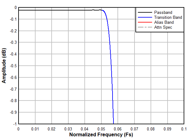 Figure 7-24 Decimation by 8 Passband Ripple Response
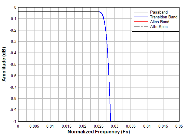 Figure 7-26 Decimation by 16 Passband Ripple Response
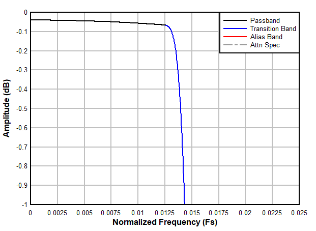 Figure 7-28 Decimation by 32 Passband Ripple Response
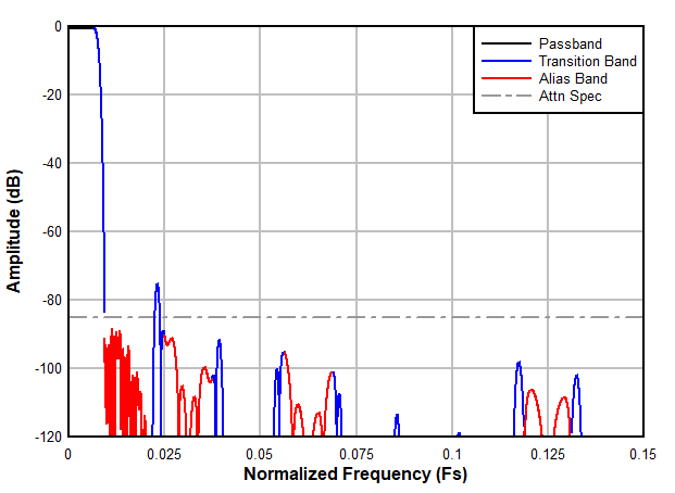 Figure 7-30 Complex Decimation by 64 Filter Response
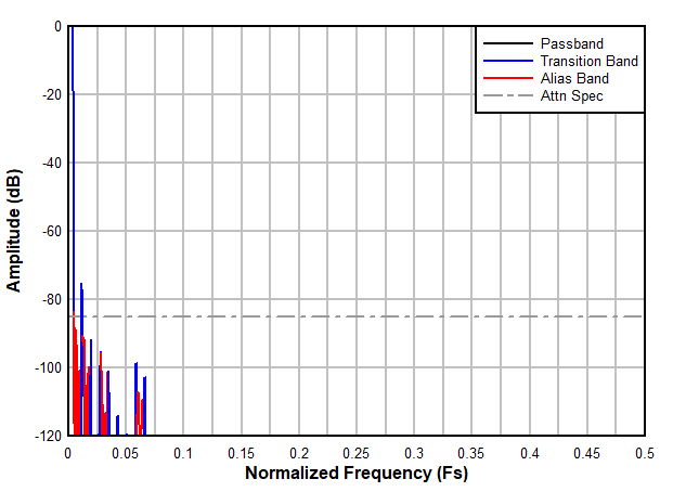 Figure 7-32 Complex Decimation by 128 Filter Response
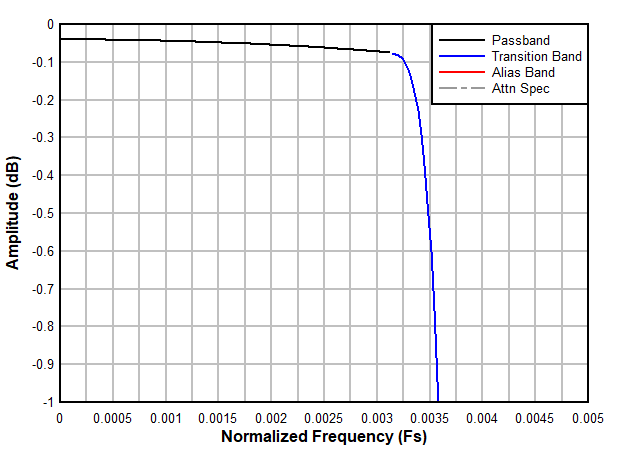 Figure 7-34 Decimation by 128 Passband Ripple Response