JAJSNQ4 March 2023 ADC34RF52
PRODUCTION DATA
- 1 特長
- 2 アプリケーション
- 3 概要
- 4 Revision History
- 5 Pin Configuration and Functions
-
6 Specifications
- 6.1 Absolute Maximum Ratings
- 6.2 ESD Ratings
- 6.3 Recommended Operating Conditions
- 6.4 Thermal Information
- 6.5 Electrical Characteristics - Power Consumption
- 6.6 Electrical Characteristics - DC Specifications
- 6.7 Electrical Characteristics - AC Specifications (Dither DISABLED)
- 6.8 Electrical Characteristics - AC Specifications (Dither ENABLED)
- 6.9 Timing Requirements
- 6.10 Typical Characteristics
-
7 Detailed Description
- 7.1 Overview
- 7.2 Functional Block Diagram
- 7.3
Feature Description
- 7.3.1 Analog Inputs
- 7.3.2 Sampling Clock Input
- 7.3.3 SYSREF
- 7.3.4 ADC Foreground Calibration
- 7.3.5 Decimation Filter
- 7.3.6 JESD204B Interface
- 7.3.7 Test Pattern
- 7.4 Device Functional Modes
- 7.5 Programming
- 7.6 Register Maps
-
8 Application Information Disclaimer
- 8.1 Application Information
- 8.2 Typical Application
- 8.3
Initialization Set Up
- 8.3.1
Initial Device Configuration After Power-Up
- 8.3.1.1 STEP 1: RESET
- 8.3.1.2 STEP 2: Device Configuration
- 8.3.1.3 STEP 3: JESD Interface Configuration (1)
- 8.3.1.4 STEP 4: SYSREF Synchronization
- 8.3.1.5 STEP 5: JESD Interface Configuration (2)
- 8.3.1.6 STEP 6: Analog Trim Settings
- 8.3.1.7 STEP 7: Calibration Configuration
- 8.3.1.8 STEP 8: SYSREF Synchronization
- 8.3.1.9 STEP 9: Run Power up Calibration
- 8.3.1.10 Step 10: JESD Interface Synchronization
- 8.3.1
Initial Device Configuration After Power-Up
- 8.4 Power Supply Recommendations
- 8.5 Layout
- 9 Device and Documentation Support
- 10Mechanical, Packaging, and Orderable Information
7.3.6.3 SERDES Output MUX
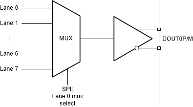
The SERDES output block contains one digital mux per SERDES output lane with a 3-bit register. This allows routing any of the 8 digital lanes to any output serdes transmitter as shown in the example for output lane DOUT0 in Figure 7-40.
 Figure 7-40 SERDES Output Mux for DOUT0
By default after power the active SERDES lanes start on lane DOUT0 as shown for the complex decimation single band example in Table 7-39. After power up the output is transmitted on lanes DOUT0..3. Using the digital output muxes, the output data for channel B is shifted from lanes DOUT2,3 to DOUT4,5. All SERDES transmitters are powered up and enabled by default. After configuring the output mux unused lanes can be powered down to save power consumption.
| OUTPUT LANE |
Default | Using MUX | ||||||
|---|---|---|---|---|---|---|---|---|
| DOUT0 | AI0 [15:8] | AI0 [7:0] | AQ0 [15:8] | AQ0 [7:0] | AI0 [15:8] | AI0 [7:0] | AQ0 [15:8] | AQ0 [7:0] |
| DOUT1 | BI0 [15:8] | BI0 [7:0] | BQ0 [15:8] | BQ0 [7:0] | BI0 [15:8] | BI0 [7:0] | BQ0 [15:8] | BQ0 [7:0] |
| DOUT2 | CI0 [15:8] | CI0 [7:0] | CQ0 [15:8] | CQ0 [7:0] | ||||
| DOUT3 | DI0 [15:8] | DI0 [7:0] | DQ0 [15:8] | DQ0 [7:0] | ||||
| DOUT4 | CI0 [15:8] | CI0 [7:0] | CQ0 [15:8] | CQ0 [7:0] | ||||
| DOUT5 | DI0 [15:8] | DI0 [7:0] | DQ0 [15:8] | DQ0 [7:0] | ||||
| DOUT6 | ||||||||
| DOUT7 | ||||||||
Table 7-40 shows the register writes to shift the output lanes from default as illustrated in Table 7-39.
| ADDR | DATA | DESCRIPTION |
|---|---|---|
| 0x05 | 0x04 | Select JESD page |
| 0x81 | 0x54 | Select internal JESD streams 4 and 5 to lanes DOUT2 and DOUT3 |
| 0x82 | 0x32 | Select internal JESD streams 2 and 3 to lanes DOUT4 and DOUT5 |