JAJSPH5 December 2022 ADC3544
PRODUCTION DATA
- 1 特長
- 2 アプリケーション
- 3 概要
- 4 Revision History
- 5 Pin Configuration and Functions
-
6 Specifications
- 6.1 Absolute Maximum Ratings
- 6.2 ESD Ratings
- 6.3 Recommended Operating Conditions
- 6.4 Thermal Information
- 6.5 Electrical Characteristics - Power Consumption
- 6.6 Electrical Characteristics - DC Specifications
- 6.7 Electrical Characteristics - AC Specifications
- 6.8 Timing Requirements
- 6.9 Typical Characteristics
- 7 Parameter Measurement Information
- 8 Detailed Description
- 9 Application Information Disclaimer
- 10Device and Documentation Support
- 11Mechanical, Packaging, and Orderable Information
パッケージ・オプション
メカニカル・データ(パッケージ|ピン)
- RSB|40
サーマルパッド・メカニカル・データ
- RSB|40
発注情報
8.3.4.4 Decimation Filter
The ADC3544 supports complex decimation by 2, 4, 8, 16 and 32 with a pass-band bandwidth of ~ 80% and a stopband rejection of at least 85 dB. Table 8-2 gives an overview of the pass-band bandwidth of the different decimation settings with respect to ADC sampling rate FS. In real decimation mode the output bandwidth is half of the complex bandwidth.
| REAL/COMPLEX DECIMATION | DECIMATION SETTING N | OUTPUT RATE | OUTPUT BANDWIDTH | OUTPUT RATE (FS = 125 MSPS) | OUTPUT BANDWIDTH (FS = 125 MSPS) |
|---|---|---|---|---|---|
| Complex | 2 | FS / 2 complex | 0.8 × FS / 2 | 62.5 MSPS complex | 50 MHz |
| 4 | FS / 4 complex | 0.8 × FS / 4 | 31.25 MSPS complex | 25 MHz | |
| 8 | FS / 8 complex | 0.8 × FS / 8 | 15.625 MSPS complex | 12.5 MHz | |
| 16 | FS / 16 complex | 0.8 × FS / 16 | 7.8125 MSPS complex | 6.25 MHz | |
| 32 | FS / 32 complex | 0.8 × FS / 32 | 3.90625 MSPS complex | 3.125 MHz | |
| Real | 2 | FS / 2 real | 0.4 × FS / 2 | 62.5 MSPS | 25 MHz |
| 4 | FS / 4 real | 0.4 × FS / 4 | 31.25 MSPS | 12.5 MHz | |
| 8 | FS / 8 real | 0.4 × FS / 8 | 15.625 MSPS | 6.25 MHz | |
| 16 | FS / 16 real | 0.4 × FS / 16 | 7.8125 MSPS | 3.125 MHz | |
| 32 | FS / 32 real | 0.4 × FS / 32 | 3.90625 MSPS | 1.5625 MHz |
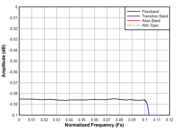
The decimation filter responses are normalized to the ADC sampling clock frequency FS and illustrated in Figure 8-19 to Figure 8-28. They are interpreted as follows:
Each figure contains the filter pass-band, transition band(s) and alias or stop-band(s) as shown in Figure 8-18. The x-axis shows the offset frequency (after the NCO frequency shift) normalized to the ADC sampling rate FS.
For example, in the divide-by-4 complex setup, the output data rate is FS / 4 complex with a Nyquist zone of FS / 8 or 0.125 × FS. The transition band (colored in blue) is centered around 0.125 × FS and the alias transition band is centered at 0.375 × FS. The stop-bands (colored in red), which alias on top of the pass-band, are centered at 0.25 × FS and 0.5 × FS. The stop-band attenuation is greater than 85 dB.
 Figure 8-18 Interpretation of the Decimation Filter Plots
 Figure 8-19 Decimation by 2 complex frequency response
 Figure 8-21 Decimation by 4 complex frequency response
 Figure 8-23 Decimation by 8 complex frequency response
 Figure 8-25 Decimation by 16 complex frequency response
 Figure 8-27 Decimation by 32 complex frequency response
 Figure 8-20 Decimation by 2 complex passband ripple response
 Figure 8-22 Decimation by 4 complex passband ripple response
 Figure 8-24 Decimation by 8 complex passband ripple response
 Figure 8-26 Decimation by 16 complex passband ripple response
 Figure 8-28 Decimation by 32 complex passband ripple response