SBASAP7 December   2024 ADC3664-SP

PRODUCTION DATA  

  1.   1
  2. Features
  3. Applications
  4. Description
  5. Pin Configuration and Functions
  6. Specifications
    1. 5.1 Absolute Maximum Ratings
    2. 5.2 ESD Ratings
    3. 5.3 Recommended Operating Conditions
    4. 5.4 Thermal Information
    5. 5.5 Electrical Characteristics - Power Consumption
    6. 5.6 Electrical Characteristics - DC Specifications
    7. 5.7 Electrical Characteristics - AC Specifications
    8. 5.8 Timing Requirements
    9. 5.9 Typical Characteristics
  7. Parameter Measurement Information
  8. Detailed Description
    1. 7.1 Overview
    2. 7.2 Functional Block Diagram
    3. 7.3 Feature Description
      1. 7.3.1 Analog Input
        1. 7.3.1.1 Analog Input Bandwidth
        2. 7.3.1.2 Analog Front End Design
          1. 7.3.1.2.1 Sampling Glitch Filter
          2. 7.3.1.2.2 AC Coupling
          3. 7.3.1.2.3 DC Coupling
      2. 7.3.2 Clock Input
        1. 7.3.2.1 Differential Vs Single-ended Clock Input
        2. 7.3.2.2 Signal Acquisition Time Adjust
      3. 7.3.3 Voltage Reference
        1. 7.3.3.1 Internal Voltage Reference
        2. 7.3.3.2 External Voltage Reference
      4. 7.3.4 Digital Data Path & Interface
        1. 7.3.4.1 Data Path Overview
        2. 7.3.4.2 Digital Interface
        3. 7.3.4.3 DCLKIN
        4. 7.3.4.4 Output Scrambler
        5. 7.3.4.5 Output Bit Mapper
          1. 7.3.4.5.1 2-Wire Mode
          2. 7.3.4.5.2 1-Wire Mode
          3. 7.3.4.5.3 1/2-Wire Mode
        6. 7.3.4.6 Output Data Format
        7. 7.3.4.7 Test Pattern
      5. 7.3.5 Digital Down Converter
        1. 7.3.5.1 Decimation Operation
        2. 7.3.5.2 Numerically Controlled Oscillator (NCO)
        3. 7.3.5.3 Decimation Filters
        4. 7.3.5.4 SYNC
        5. 7.3.5.5 Output Data Format with Decimation
    4. 7.4 Device Functional Modes
      1. 7.4.1 Low Latency Mode
      2. 7.4.2 Averaging Mode
    5. 7.5 Programming
      1. 7.5.1 Pin Control
      2. 7.5.2 Serial Peripheral Interface (SPI)
        1. 7.5.2.1 Register Write
        2. 7.5.2.2 Register Read
      3. 7.5.3 Device Configuration Steps
      4. 7.5.4 Register Map
        1. 7.5.4.1 Detailed Register Description
  9. Application Information Disclaimer
    1. 8.1 Application Information
    2. 8.2 Typical Application
      1. 8.2.1 Design Requirements
      2. 8.2.2 Detailed Design Procedure
    3. 8.3 Initialization Set Up
    4. 8.4 Power Supply Recommendations
    5. 8.5 Layout
      1. 8.5.1 Layout Guidelines
      2. 8.5.2 Layout Example
  10. Device and Documentation Support
    1. 9.1 Receiving Notification of Documentation Updates
    2. 9.2 Support Resources
    3. 9.3 Trademarks
    4. 9.4 Electrostatic Discharge Caution
    5. 9.5 Glossary
  11. 10Revision History
  12. 11Mechanical, Packaging, and Orderable Information
    1. 11.1 Mechanical Data

パッケージ・オプション

デバイスごとのパッケージ図は、PDF版データシートをご参照ください。

メカニカル・データ(パッケージ|ピン)
  • HBP|64
サーマルパッド・メカニカル・データ
発注情報

Power Supply Recommendations

The ADC3664-SP requires two different power supplies. The AVDD supply provides power for the internal analog circuits and to the ADC while the IOVDD supply powers the digital interface and the internal digital circuits. Power sequencing is not required.

A low noise power supply should supply the AVDD rail to achieve data sheet performance.

There are two recommended power-supply architectures:

  1. A high efficiency switching regulator followed by a low noise LDO to suppress the switching noise and improve voltage accuracy.
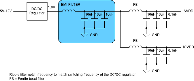
  2. Directly step down to the final ADC supply voltage using a high efficiency switching regulator. This approach provides the best efficiency; however, care must be taken to make sure the switching regulator noise doesnot degrade the ADC performance.

The TPS7H4002-SP is recommended as the first stage radiation hardened switching regulator. The switching regulator can be followed by either the TPS7A4501-SP or the TPS7H1111-SP which are both space hardened LDOs.

Note: AVDD and IOVDD supply voltages should not be shared to prevent digital switching noise from coupling into the analog signal chain.
ADC3664-SP Example LDO Based
                    ApproachFigure 8-2 Example LDO Based Approach
ADC3664-SP Example Switcher Only
                    ApproachFigure 8-3 Example Switcher Only Approach