SBASAP7 December 2024 ADC3664-SP
PRODUCTION DATA
- 1
- 1 Features
- 2 Applications
- 3 Description
- 4 Pin Configuration and Functions
-
5 Specifications
- 5.1 Absolute Maximum Ratings
- 5.2 ESD Ratings
- 5.3 Recommended Operating Conditions
- 5.4 Thermal Information
- 5.5 Electrical Characteristics - Power Consumption
- 5.6 Electrical Characteristics - DC Specifications
- 5.7 Electrical Characteristics - AC Specifications
- 5.8 Timing Requirements
- 5.9 Typical Characteristics
- 6 Parameter Measurement Information
- 7 Detailed Description
- 8 Application Information Disclaimer
- 9 Device and Documentation Support
- 10Revision History
- 11Mechanical, Packaging, and Orderable Information
パッケージ・オプション
デバイスごとのパッケージ図は、PDF版データシートをご参照ください。
メカニカル・データ(パッケージ|ピン)
- HBP|64
サーマルパッド・メカニカル・データ
発注情報
7.3.5.3 Decimation Filters
Table 7-5 provides an overview of the passband bandwidths and output data rates of the different decimation settings with respect to the ADC sampling rate FS.
Table 7-5 Decimation Filter Summary and Maximum
Available Output Bandwidth
| REAL/COMPLEX DECIMATION | DECIMATION SETTING N | OUTPUT RATE | OUTPUT BANDWIDTH | OUTPUT RATE (FS = 65 MSPS) | OUTPUT BANDWIDTH (FS = 65 MSPS) |
|---|---|---|---|---|---|
| Complex | 2 | FS / 2 complex | 0.8 × FS / 2 | 32.5 MSPS complex | 26 MHz |
| 4 | FS / 4 complex | 0.8 × FS / 4 | 16.25 MSPS complex | 13 MHz | |
| 8 | FS / 8 complex | 0.8 × FS / 8 | 8.125 MSPS complex | 6.5 MHz | |
| 16 | FS / 16 complex | 0.8 × FS / 16 | 4.0625 MSPS complex | 3.25 MHz | |
| 32 | FS / 32 complex | 0.8 × FS / 32 | 2.03125 MSPS complex | 1.625 MHz | |
| Real | 2 | FS / 2 | 0.4 × FS / 2 | 32.5 MSPS | 13 MHz |
| 4 | FS / 4 | 0.4 × FS / 4 | 16.25 MSPS | 6.5 MHz | |
| 8 | FS / 8 | 0.4 × FS / 8 | 8.125 MSPS | 3.25 MHz | |
| 16 | FS / 16 | 0.4 × FS / 16 | 4.0625 MSPS | 1.625 MHz | |
| 32 | FS / 32 | 0.4 × FS / 32 | 2.03125 MSPS | 0.8125 MHz |
The decimation filter responses are normalized to the ADC sampling clock frequency FS and illustrated in Figure 7-20 to Figure 7-29. Each figure contains the filter passband, transition band(s) and stopband(s).
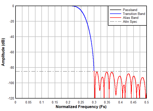 Figure 7-20 Decimation by 2 Filter Frequency
Response
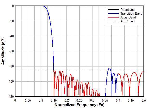 Figure 7-22 Decimation by 4 Filter Frequency
Response
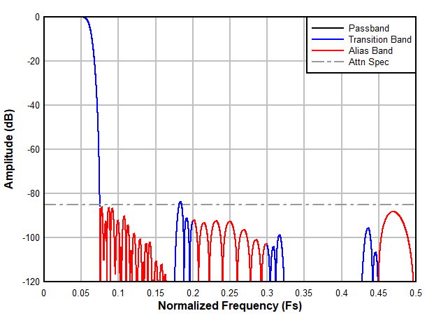 Figure 7-24 Decimation by 8 Filter Frequency
Response
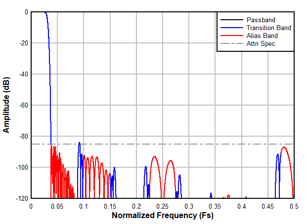 Figure 7-26 Decimation by 16 Filter Frequency
Response
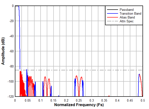 Figure 7-28 Decimation by 32 Filter Frequency
Response
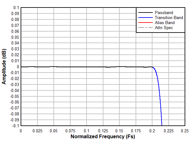 Figure 7-21 Decimation by 2 Filter Passband
Ripple Response
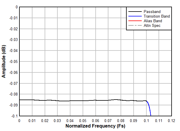 Figure 7-23 Decimation by 4 Filter Passband
Ripple Response
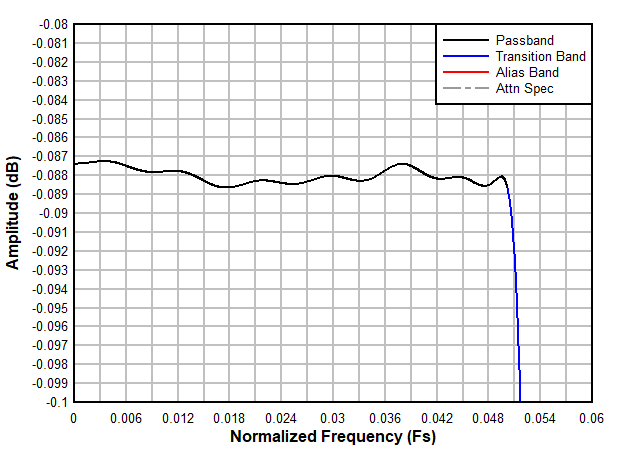 Figure 7-25 Decimation by 8 Filter Passband
Ripple Response
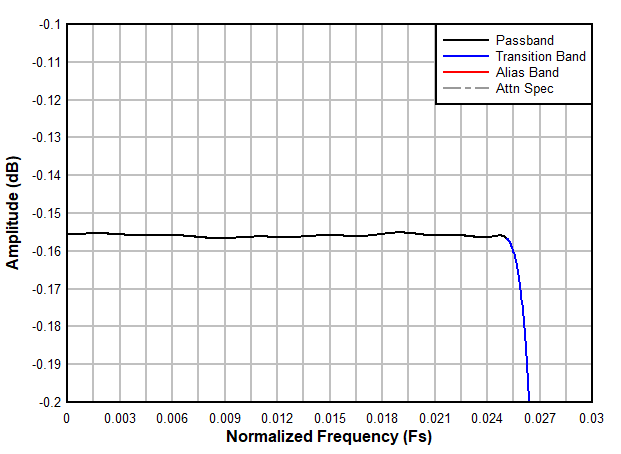 Figure 7-27 Decimation by 16 Filter Passband
Ripple Response
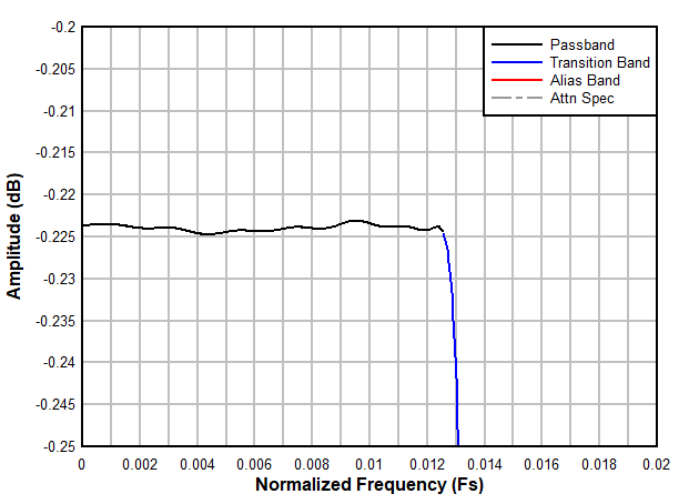 Figure 7-29 Decimation by 32 Filter Passband
Ripple Response