JAJSLC0 March   2024 ADC3683-SP

PRODMIX  

  1.   1
  2. 特長
  3. アプリケーション
  4. 概要
  5. Pin Configuration and Functions
  6. Specifications
    1. 5.1 Absolute Maximum Ratings
    2. 5.2 ESD Ratings
    3. 5.3 Recommended Operating Conditions
    4. 5.4 Thermal Information
    5. 5.5 Electrical Characteristics - Power Consumption
    6. 5.6 Electrical Characteristics - DC Specifications
    7. 5.7 Electrical Characteristics - AC Specifications
    8. 5.8 Timing Requirements
    9. 5.9 Typical Characteristics
  7. Parameter Measurement Information
  8. Detailed Description
    1. 7.1 Overview
    2. 7.2 Functional Block Diagram
    3. 7.3 Feature Description
      1. 7.3.1 Analog Input
        1. 7.3.1.1 Analog Front End Design
          1. 7.3.1.1.1 Sampling Glitch Filter Design
          2. 7.3.1.1.2 Analog Input Termination and DC Bias
            1. 7.3.1.1.2.1 AC-Coupling
            2. 7.3.1.1.2.2 DC-Coupling
        2. 7.3.1.2 Auto-Zero Feature
      2. 7.3.2 Clock Input
        1. 7.3.2.1 Single Ended vs Differential Clock Input
        2. 7.3.2.2 Signal Acquisition Time Adjust
      3. 7.3.3 Voltage Reference
        1. 7.3.3.1 Internal Voltage Reference
        2. 7.3.3.2 External Voltage Reference (VREF)
        3. 7.3.3.3 External Voltage Reference with Internal Buffer (REFBUF)
      4. 7.3.4 Digital Down Converter
        1. 7.3.4.1 DDC MUX
        2. 7.3.4.2 Digital Filter Operation
        3. 7.3.4.3 FS/4 Mixing with Real Output
        4. 7.3.4.4 Numerically Controlled Oscillator (NCO) and Digital Mixer
        5. 7.3.4.5 Decimation Filter
        6. 7.3.4.6 SYNC
        7. 7.3.4.7 Output Formatting with Decimation
      5. 7.3.5 Digital Interface
        1. 7.3.5.1 Output Formatter
        2. 7.3.5.2 Output Scrambler
        3. 7.3.5.3 Output Bit Mapper
          1. 7.3.5.3.1 2-Wire Mode
          2. 7.3.5.3.2 1-Wire Mode
          3. 7.3.5.3.3 ½-Wire Mode
        4. 7.3.5.4 Output Interface or Mode Configuration
          1. 7.3.5.4.1 Configuration Example
        5. 7.3.5.5 Output Data Format
      6. 7.3.6 Test Pattern
    4. 7.4 Device Functional Modes
      1. 7.4.1 Normal Operation
      2. 7.4.2 Power Down Options
      3. 7.4.3 Digital Channel Averaging
    5. 7.5 Programming
      1. 7.5.1 Configuration using PINs only
      2. 7.5.2 Configuration using the SPI interface
        1. 7.5.2.1 Register Write
        2. 7.5.2.2 Register Read
  9. Application Information Disclaimer
    1. 8.1 Application Information
    2. 8.2 Typical Application
      1. 8.2.1 Design Requirements
      2. 8.2.2 Detailed Design Procedure
        1. 8.2.2.1 Input Signal Path
        2. 8.2.2.2 Sampling Clock
        3. 8.2.2.3 Voltage Reference
      3. 8.2.3 Application Curves
    3. 8.3 Initialization Set Up
      1. 8.3.1 Register Initialization During Operation
    4. 8.4 Power Supply Recommendations
    5. 8.5 Layout
      1. 8.5.1 Layout Guidelines
      2. 8.5.2 Layout Example
  10. Register Map
    1. 9.1 Detailed Register Description
  11. 10Device and Documentation Support
    1. 10.1 ドキュメントの更新通知を受け取る方法
    2. 10.2 サポート・リソース
    3. 10.3 Trademarks
    4. 10.4 静電気放電に関する注意事項
    5. 10.5 用語集
  12. 11Revision History
  13. 12Mechanical, Packaging, and Orderable Information
    1. 12.1 Mechanical Data

パッケージ・オプション

メカニカル・データ(パッケージ|ピン)
サーマルパッド・メカニカル・データ
発注情報
Sampling Glitch Filter Design

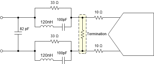
The front end sampling glitch filter is designed to optimize the SNR and HD3 performance of the ADC. The filter performance is dependent on input frequency: therefore, the following filter designs are recommended for different input frequency ranges as shown in Figure 7-2 and Figure 7-3 (assuming a 50Ω source impedance).
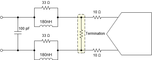
GUID-814446D6-B655-43C2-A093-51FA97D5B30F-low.gifFigure 7-2 Sampling Glitch Filter Example for Input Frequencies From DC to 30MHz
GUID-71374044-E383-456C-87C1-85BEAB9032A4-low.gifFigure 7-3 Sampling Glitch Filter Example for Input Frequencies From 30 to 70MHz