JAJSKW0B December 2020 – October 2022 ADC3681 , ADC3682 , ADC3683
PRODUCTION DATA
- 1 特長
- 2 アプリケーション
- 3 概要
- 4 Revision History
- 5 Pin Configuration and Functions
-
6 Specifications
- 6.1 Absolute Maximum Ratings
- 6.2 ESD Ratings
- 6.3 Recommended Operating Conditions
- 6.4 Thermal Information
- 6.5 Electrical Characteristics - Power Consumption
- 6.6 Electrical Characteristics - DC Specifications
- 6.7 Electrical Characteristics - AC Specifications
- 6.8 Timing Requirements
- 6.9 Typical Characteristics - ADC3681
- 6.10 Typical Characteristics - ADC3682
- 6.11 Typical Characteristics - ADC3683
- 7 Parameter Measurement Information
- 8 Detailed Description
- 9 Application Information Disclaimer
- 10Device and Documentation Support
- 11Mechanical, Packaging, and Orderable Information
パッケージ・オプション
メカニカル・データ(パッケージ|ピン)
- RSB|40
サーマルパッド・メカニカル・データ
- RSB|40
発注情報
8.4.2 Power Down Options
A global power down mode can be enabled via SPI as well as using the power down pin (PDN/SYNC). There is an internal pull-down 21 kΩ resistor on the PDN/SYNC input pin and the pin is active high - so the pin needs to be pulled high externally to enter global power down mode.
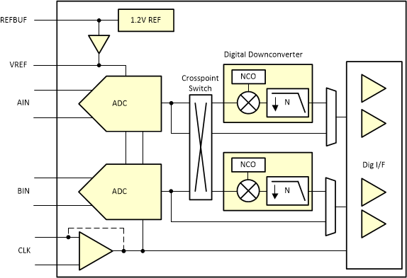
The SPI register map provides the capability to enable/disable individual blocks directly or via PDN pin mask in order to trade off power consumption vs wake up time as shown in Table 8-10.
 Figure 8-49 Power Down Configurations
Table 8-10 Overview of Power Down Options
| Function/ Register | PDN via SPI | Mask for Global PDN | Feature - Default | Power Impact | Wake-up time | Comment |
|---|---|---|---|---|---|---|
| ADC | Yes | - | Enabled | Both ADC channels are included in Global PDN automatically | ||
| Reference gain amplifier | Yes | Yes | Enabled | ~ 0.4 mA | ~3 us | Should only be powered down in power down state. |
| Internal 1.2V reference | Yes | External ref | ~ 1-3.5 mA | ~3 ms | Internal/external reference selection is available through SPI and REFBUF pin. | |
| Clock buffer | Yes | Differential clock | ~ 1 mA | n/a | Single ended clock input saves ~ 1mA compared to differential. Some programmability is available through the REFBUF pin. | |
| Output interface drivers | Yes | - | Enabled | varies | n/a | Depending on output interface mode, unused output drivers can be powered down for maximum power savings |
| Decimation filter | Yes | - | Disabled | see electrical table | n/a |