JAJSA35G April 2003 – May 2016 ADCS7476 , ADCS7477 , ADCS7478
PRODUCTION DATA.
9 Power Supply Recommendations
There are three concerns relating to the power supply of these products: the effects of Power Supply Noise upon the conversion process, the Digital Output Effect Upon Noise upon the conversion process, and Power Management of the product.
9.1 Power Supply Noise
Because the supply voltage of the ADCS747x is the reference voltage, any noise greater than 1/2 LSB in amplitude has some effect upon the converter noise performance. This effect is proportional to the input voltage level. The power supply must receive all the considerations of a reference voltage as far as stability and noise is concerned. Using the same supply voltage for these devices as is used for digital components leads to degraded noise performance.
9.2 Digital Output Effect Upon Noise
The charging of any output load capacitance requires current from the digital supply, VDD. The current pulses required from the supply to charge the output capacitance causes voltage variations at the ADC supply line. If these variations are large enough, they could degrade SNR and SINAD performance of the ADC. Similarly, discharging the output capacitance when the digital output goes from a logic high to a logic low dumps current into the die substrate, causing ground bounce noise in the substrate that degrades noise performance if that current is large enough. The larger the output capacitance, the more current flows through the device power supply line and die substrate and the greater is the noise coupled into the analog path.
The first solution to keeping digital noise out of the power supply is to decouple the supply from any other components or use a separate supply for the ADC. To keep noise out of the supply, keep the output load capacitance as small as practical. If the load capacitance is greater than 50 pF, use a 100-Ω series resistor at the ADC output, located as close to the ADC output pin as practical. This limits the charge and discharge current of the output capacitance and improve noise performance. Because the series resistor and the load capacitance form a low frequency pole, verify signal integrity when the series resistor is added.
9.3 Power Management
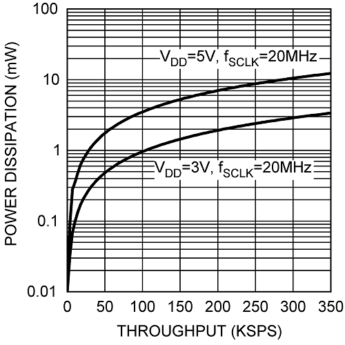
When ADCS747x is operated continuously in normal mode, throughput up to 1 MSPS can be achieved. The user may trade throughput for power consumption by simply performing fewer conversions per unit time and putting the ADCS747x into shutdown mode between conversions. This method is not advantageous beyond 350-kSPS throughput.
A plot of maximum power consumption versus throughput is shown in Figure 35. To calculate the power consumption for a given throughput, remember that each time the part exits shutdown mode and enters normal mode, one dummy conversion is required. Generally, the user puts the part into normal mode, execute one dummy conversion followed by one valid conversion, and then put the part back into shutdown mode. When this is done, the fraction of time spent in normal mode may be calculated by multiplying the throughput (in samples per second) by 2 µs, the time taken to perform one dummy and one valid conversion. The power consumption can then be found by multiplying the fraction of time spent in normal mode by the normal mode power consumption figure. The power dissipated while the part is in shutdown mode is negligible.
For example, to calculate the power consumption at 300 kSPS with VDD = 5 V, begin by calculating the fraction of time spent in normal mode: 300,000 samples/second x 2 µs = 0.6, or 60%. The power consumption at 300 kSPS is then 60% of 17.5 mW (the maximum power consumption at VDD = 5 V) or 10.5 mW.
 Figure 35. Maximum Power Consumption vs Throughput