JAJSA35G April 2003 – May 2016 ADCS7476 , ADCS7477 , ADCS7478
PRODUCTION DATA.
6 Specifications
6.1 Absolute Maximum Ratings
over operating free-air temperature range (unless otherwise noted)(1)(2)| MIN | MAX | UNIT | ||
|---|---|---|---|---|
| Supply voltage, VDD | –0.3 | 6.5 | V | |
| Voltage on any analog pin to GND | –0.3 | VDD + 0.3 | V | |
| Voltage on any digital pin to GND | –0.3 | 6.5 | V | |
| Input current at any pin (except power supply pins) | ±10 | mA | ||
| Soldering temperature, infrared (10 sec) | 215 | °C | ||
| Operating temperature, TA | 150 | °C | ||
| Storage temperature, Tstg | –65 | 150 | °C | |
(1) Stresses beyond those listed under Absolute Maximum Ratings may cause permanent damage to the device. These are stress ratings only, which do not imply functional operation of the device at these or any other conditions beyond those indicated under Recommended Operating Conditions. Exposure to absolute-maximum-rated conditions for extended periods may affect device reliability.
(2) If Military/Aerospace specified devices are required, please contact the Texas Instruments Sales Office/ Distributors for availability and specifications.
6.2 ESD Ratings
| VALUE | UNIT | |||
|---|---|---|---|---|
| V(ESD) | Electrostatic discharge | Human-body model (HBM), per ANSI/ESDA/JEDEC JS-001(1) | ±3500 | V |
| Charged-device model (CDM), per JEDEC specification JESD22-C101(2) | ±200 | |||
(1) JEDEC document JEP155 states that 500-V HBM allows safe manufacturing with a standard ESD control process.
(2) JEDEC document JEP157 states that 250-V CDM allows safe manufacturing with a standard ESD control process.
6.3 Recommended Operating Conditions
over operating free-air temperature range (unless otherwise noted)| MIN | MAX | UNIT | ||
|---|---|---|---|---|
| VDD | Supply voltage | 2.7 | 5.25 | V |
| Digital input pins voltage (independent of supply voltage) | 2.7 | 5.25 | V | |
| TA | Operating temperature | –40 | 125 | °C |
6.4 Thermal Information
| THERMAL METRIC(1) | ADCS7476, ADCS7477, ADCS7478 | UNIT | |
|---|---|---|---|
| DBV (SOT-23) | |||
| 6 PINS | |||
| RθJA | Junction-to-ambient thermal resistance | 184.5 | °C/W |
| RθJC(top) | Junction-to-case (top) thermal resistance | 151.2 | °C/W |
| RθJB | Junction-to-board thermal resistance | 29.7 | °C/W |
| ψJT | Junction-to-top characterization parameter | 29.8 | °C/W |
| ψJB | Junction-to-board characterization parameter | 29.1 | °C/W |
(1) For more information about traditional and new thermal metrics, see the Semiconductor and IC Package Thermal Metrics application report, SPRA953.
6.5 Electrical Characteristics – ADCS7476
TA = 25°C, VDD = 2.7 V to 5.25 V, fSCLK = 20 MHz, and fSAMPLE = 1 MSPS (unless otherwise noted)(1)(1) Data sheet minimum and maximum specification limits are ensured by design, test, or statistical analysis.
6.6 Electrical Characteristics – ADCS7477
TA = 25°C, VDD = 2.7 V to 5.25 V, fSCLK = 20 MHz, and fSAMPLE = 1 MSPS (unless otherwise noted)(1)| PARAMETER | TEST CONDITIONS | MIN | TYP | MAX | UNIT | ||
|---|---|---|---|---|---|---|---|
| STATIC CONVERTER CHARACTERISTICS | |||||||
| Resolution with no missing codes | –40°C ≤ TA ≤ 85°C | 10 | Bits | ||||
| INL | Integral non-linearity | TA = 25°C | ±0.2 | LSB | |||
| –40°C ≤ TA ≤ 85°C | ±0.7 | ||||||
| DNL | Differential non-linearity | TA = 25°C | –0.2 | 0.3 | LSB | ||
| T–40°C ≤ TA ≤ 85°C | ±0.7 | ±0.7 | |||||
| VOFF | Offset error | TA = 25°C | ±0.1 | LSB | |||
| –40°C ≤ TA ≤ 85°C | ±0.7 | ||||||
| GE | Gain error | TA = 25°C | ±0.2 | LSB | |||
| –40°C ≤ TA ≤ 85°C | ±1 | ||||||
| DYNAMIC CONVERTER CHARACTERISTICS | |||||||
| SINAD | Signal-to-noise plus distortion ratio | fIN = 100 kHz | TA = 25°C | 61.7 | dBFS | ||
| –40°C ≤ TA ≤ 85°C | 61 | ||||||
| SNR | Signal-to-noise ratio | fIN = 100 kHz | 62 | dB | |||
| THD | Total harmonic distortion | fIN = 100 kHz | TA = 25°C | –77 | dB | ||
| –40°C ≤ TA ≤ 85°C | –73 | ||||||
| SFDR | Spurious-free dynamic range | fIN = 100 kHz | TA = 25°C | 78 | dB | ||
| –40°C ≤ TA ≤ 85°C | 74 | ||||||
| IMD | Intermodulation distortion, second order terms |
fa = 103.5 kHz, fb = 113.5 kHz | –78 | dB | |||
| Intermodulation distortion, third order terms |
fa = 103.5 kHz, fb = 113.5 kHz | –78 | dB | ||||
| FPBW | –3-dB full power bandwidth | 5-V supply | 11 | MHz | |||
| 3-V supply | 8 | MHz | |||||
| POWER SUPPLY CHARACTERISTICS | |||||||
| IDD | Normal mode (static) | VDD = 4.75 V to 5.25 V, SCLK On or Off | 2 | mA | |||
| VDD = 2.7 V to 3.6 V, SCLK On or Off | 1 | mA | |||||
| Normal mode (operational) | VDD = 4.75 V to 5.25 V, fSAMPLE = 1 MSPS |
TA = 25°C | 2 | mA | |||
| –40°C ≤ TA ≤ 85°C | 3.5 | ||||||
| VDD = 2.7 V to 3.6 V, fSAMPLE = 1 MSPS |
TA = 25°C | 0.6 | mA | ||||
| –40°C ≤ TA ≤ 85°C | 1.6 | ||||||
| Shutdown mode | VDD = 5 V, SCLK Off | 0.5 | µA | ||||
| VDD = 5 V, SCLK On | 60 | ||||||
| PD | Power consumption, normal mode (operational) |
VDD = 5 V, fSAMPLE = 1 MSPS |
TA = 25°C | 10 | mW | ||
| –40°C ≤ TA ≤ 85°C | 17.5 | ||||||
| VDD = 3 V, fSAMPLE = 1 MSPS |
TA = 25°C | 2 | mW | ||||
| –40°C ≤ TA ≤ 85°C | 4.8 | ||||||
| Power consumption, shutdown mode |
VDD = 5 V, SCLK Off | 2.5 | µW | ||||
| VDD = 3 V, SCLK Off | 1.5 | ||||||
| ANALOG INPUT CHARACTERISTICS | |||||||
| VIN | Input range | 0 to VDD | V | ||||
| IDCL | DC leakage current | TA = −40°C to 85°C | ±1 | µA | |||
| CINA | Analog input capacitance | 30 | pF | ||||
| DIGITAL INPUT CHARACTERISTICS | |||||||
| VIH | Input high voltage | TA = −40°C to 85°C | 2.4 | V | |||
| VIL | Input low voltage | VDD = 5 V, –40°C ≤ TA ≤ 85°C | 0.8 | V | |||
| VDD = 3 V, –40°C ≤ TA ≤ 85°C | 0.4 | V | |||||
| IIN | Input current | VIN = 0 V or VDD | TA = 25°C | ±10 | nA | ||
| –40°C ≤ TA ≤ 85°C | ±1 | µA | |||||
| CIND | Digital input capacitance | TA = 25°C | 2 | pF | |||
| –40°C ≤ TA ≤ 85°C | 4 | ||||||
| DIGITAL OUTPUT CHARACTERISTICS | |||||||
| VOH | Output high voltage | ISOURCE = 200 µA, VDD = 2.7 V to 5.25 V, –40°C ≤ TA ≤ 85°C |
VDD – 0.2 | V | |||
| VOL | Output low voltage | ISINK = 200 µA, –40°C ≤ TA ≤ 85°C | 0.4 | V | |||
| IOL | TRI-STATE leakage current | –40°C ≤ TA ≤ 85°C | ±10 | µA | |||
| COUT | TRI-STATE output capacitance | TA = 25°C | 2 | pF | |||
| –40°C ≤ TA ≤ 85°C | 4 | ||||||
| Output coding | Straight (natural) binary | ||||||
| AC ELECTRICAL CHARACTERISTICS | |||||||
| fSCLK | Clock frequency | –40°C ≤ TA ≤ 85°C | 20 | MHz | |||
| DC | SCLK duty cycle | –40°C ≤ TA ≤ 85°C | 40% | 60% | |||
| tTH | Track or hold acquisition time | –40°C ≤ TA ≤ 85°C | 400 | ns | |||
| fRATE | Throughput rate | –40°C ≤ TA ≤ 85°C | 1 | MSPS | |||
| tAD | Aperture delay | 3 | ns | ||||
| tAJ | Aperture jitter | 30 | ps | ||||
(1) Data sheet minimum and maximum specification limits are ensured by design, test, or statistical analysis.
6.7 Electrical Characteristics – ADCS7478
TA = 25°C, VDD = 2.7 V to 5.25 V, fSCLK = 20 MHz, and fSAMPLE = 1 MSPS (unless otherwise noted)(1)| PARAMETER | TEST CONDITIONS | MIN | TYP | MAX | UNIT | ||
|---|---|---|---|---|---|---|---|
| STATIC CONVERTER CHARACTERISTICS | |||||||
| Resolution with no missing codes | –40°C ≤ TA ≤ 85°C | 8 | Bits | ||||
| INL | Integral non-linearity | TA = 25°C | ±0.05 | LSB | |||
| –40°C ≤ TA ≤ 85°C | ±0.3 | ||||||
| DNL | Differential non-linearity | TA = 25°C | ±0.07 | LSB | |||
| –40°C ≤ TA ≤ 85°C | ±0.3 | ||||||
| VOFF | Offset error | TA = 25°C | ±0.03 | LSB | |||
| –40°C ≤ TA ≤ 85°C | ±0.3 | ||||||
| GE | Gain error | TA = 25°C | ±0.08 | LSB | |||
| –40°C ≤ TA ≤ 85°C | ±0.4 | ||||||
| Total unadjusted error | TA = 25°C | ±0.07 | LSB | ||||
| –40°C ≤ TA ≤ 85°C | ±0.3 | ||||||
| DYNAMIC CONVERTER CHARACTERISTICS | |||||||
| SINAD | Signal-to-noise plus distortion ratio | fIN = 100 kHz | TA = 25°C | 49.7 | dB | ||
| –40°C ≤ TA ≤ 85°C | 49 | ||||||
| SNR | Signal-to-noise ratio | fIN = 100 kHz | 49.7 | dB | |||
| THD | Total harmonic distortion | fIN = 100 kHz | TA = 25°C | –77 | dB | ||
| –40°C ≤ TA ≤ 85°C | –65 | ||||||
| SFDR | Spurious-free dynamic range | fIN = 100 kHz | TA = 25°C | 69 | dB | ||
| –40°C ≤ TA ≤ 85°C | 65 | ||||||
| IMD | Intermodulation distortion, second order terms |
fa = 103.5 kHz, fb = 113.5 kHz | –68 | dB | |||
| Intermodulation distortion, third order terms |
fa = 103.5 kHz, fb = 113.5 kHz | –68 | dB | ||||
| FPBW | –3-dB full power bandwidth | 5-V supply | 11 | MHz | |||
| 3-V supply | 8 | MHz | |||||
| POWER SUPPLY CHARACTERISTICS | |||||||
| IDD | Normal mode (static) | VDD = 4.75 V to 5.25 V, SCLK On or Off | 2 | mA | |||
| VDD = 2.7 V to 3.6 V, SCLK On or Off | 1 | mA | |||||
| Normal mode (operational) | VDD = 4.75 V to 5.25 V, fSAMPLE = 1 MSPS |
TA = 25°C | 2 | mA | |||
| –40°C ≤ TA ≤ 85°C | 3.5 | ||||||
| VDD = 2.7 V to 3.6 V, fSAMPLE = 1 MSPS |
TA = 25°C | 0.6 | mA | ||||
| –40°C ≤ TA ≤ 85°C | 1.6 | ||||||
| Shutdown mode | VDD = 5 V, SCLK Off | 0.5 | µA | ||||
| VDD = 5 V, SCLK On | 60 | ||||||
| PD | Power consumption, normal mode (operational) |
VDD = 5 V, fSAMPLE = 1 MSPS |
TA = 25°C | 10 | mW | ||
| –40°C ≤ TA ≤ 85°C | 17.5 | ||||||
| VDD = 3 V, fSAMPLE = 1 MSPS |
TA = 25°C | 2 | mW | ||||
| –40°C ≤ TA ≤ 85°C | 4.8 | ||||||
| Power consumption, shutdown mode |
VDD = 5 V, SCLK Off | 2.5 | µW | ||||
| VDD = 3 V, SCLK Off | 1.5 | ||||||
| ANALOG INPUT CHARACTERISTICS | |||||||
| VIN | Input range | 0 to VDD | V | ||||
| IDCL | DC leakage current | –40°C ≤ TA ≤ 85°C | ±1 | µA | |||
| CINA | Analog input capacitance | 30 | pF | ||||
| DIGITAL INPUT CHARACTERISTICS | |||||||
| VIH | Input high voltage | –40°C ≤ TA ≤ 85°C | 2.4 | V | |||
| VIL | Input low voltage | VDD = 5 V, –40°C ≤ TA ≤ 85°C | 0.8 | V | |||
| VDD = 3 V, –40°C ≤ TA ≤ 85°C | 0.4 | V | |||||
| IIN | Digital input current | VIN = 0 V or VDD | TA = 25°C | ±10 | nA | ||
| –40°C ≤ TA ≤ 85°C | ±1 | µA | |||||
| CIND | Input capacitance | TA = 25°C | 2 | p | |||
| –40°C ≤ TA ≤ 85°C | 4 | ||||||
| DIGITAL OUTPUT CHARACTERISTICS | |||||||
| VOH | Output high voltage | ISOURCE = 200 µA, VDD = 2.7 V to 5.25 V, –40°C ≤ TA ≤ 85°C |
VDD − 0.2 | V | |||
| VOL | Output low voltage | ISINK = 200 µA, –40°C ≤ TA ≤ 85°C | 0.4 | V | |||
| IOL | TRI-STATE leakage current | –40°C ≤ TA ≤ 85°C | ±10 | µA | |||
| COUT | TRI-STATE output capacitance | 2 | 4 | pF | |||
| Output coding | Straight (natural) binary | ||||||
| AC ELECTRICAL CHARACTERISTICS | |||||||
| fSCLK | Clock frequency | –40°C ≤ TA ≤ 85°C | 20 | MHz | |||
| DC | SCLK duty cycle | –40°C ≤ TA ≤ 85°C | 40% | 60% | |||
| tTH | Track or hold acquisition time | –40°C ≤ TA ≤ 85°C | 400 | ns | |||
| fRATE | Throughput rate | –40°C ≤ TA ≤ 85°C (see Application Information) | 1 | MSPS | |||
| tAD | Aperture delay | 3 | ns | ||||
| tAJ | Aperture jitter | 30 | ps | ||||
(1) Data sheet min/max specification limits are ensured by design, test, or statistical analysis.
6.8 Timing Requirements
–40°C ≤ TA ≤ 85°C, VDD = 2.7 V to 5.25 V, and fSCLK = 20 MHz (unless otherwise noted)(1)| PARAMETER | CONDITIONS | MIN | TYP | MAX | UNIT | |
|---|---|---|---|---|---|---|
| tCONVERT | TA = 25°C | 16 × tSCLK | ||||
| tQUIET | Quiet time(2) | 50 | ns | |||
| t1 | Minimum CS pulse width | 10 | ns | |||
| t2 | CS to SCLK setup time | 10 | ns | |||
| t3 | Delay from CS until SDATA TRI-STATE disabled (3) | 20 | ns | |||
| t4 | Data access time after SCLK falling edge(4) | VDD = 2.7 V to 3.6 V | 40 | ns | ||
| VDD = 4.75 V to 5.25 V | 20 | ns | ||||
| t5 | SCLK low pulse width | 0.4 × tSCLK | ns | |||
| t6 | SCLK high pulse width | 0.4 × tSCLK | ns | |||
| t7 | SCLK to data valid hold time | VDD = 2.7 V to 3.6 V | 7 | ns | ||
| VDD = 4.75 V to 5.25 V | 5 | ns | ||||
| t8 | SCLK falling edge to SDATA high impedance (5) | VDD = 2.7 V to 3.6 V | 6 | 25 | ns | |
| VDD = 4.75 V to 5.25 V | 5 | 25 | ns | |||
| tPOWER-UP | Power-up time from full power down | TA = 25°C | 1 | µs | ||
(1) All input signals are specified as tr = tf = 5 ns (10% to 90% VDD) and timed from 1.6 V.
(2) Minimum quiet time required between bus relinquish and start of next conversion.
(3) Measured with the load circuit (Figure 1), and defined as the time taken by the output to cross 1 V.
(4) Measured with the load circuit (Figure 1), and defined as the time taken by the output to cross 1 V or 2 V.
(5) t8 is derived from the time taken by the outputs to change by 0.5 V with the loading circuit (Figure 1). The measured number is then adjusted to remove the effects of charging or discharging the 25-pF capacitor. This means t8 is the true bus relinquish time, independent of the bus loading.
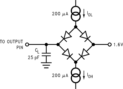 Figure 1. Timing Test Circuit
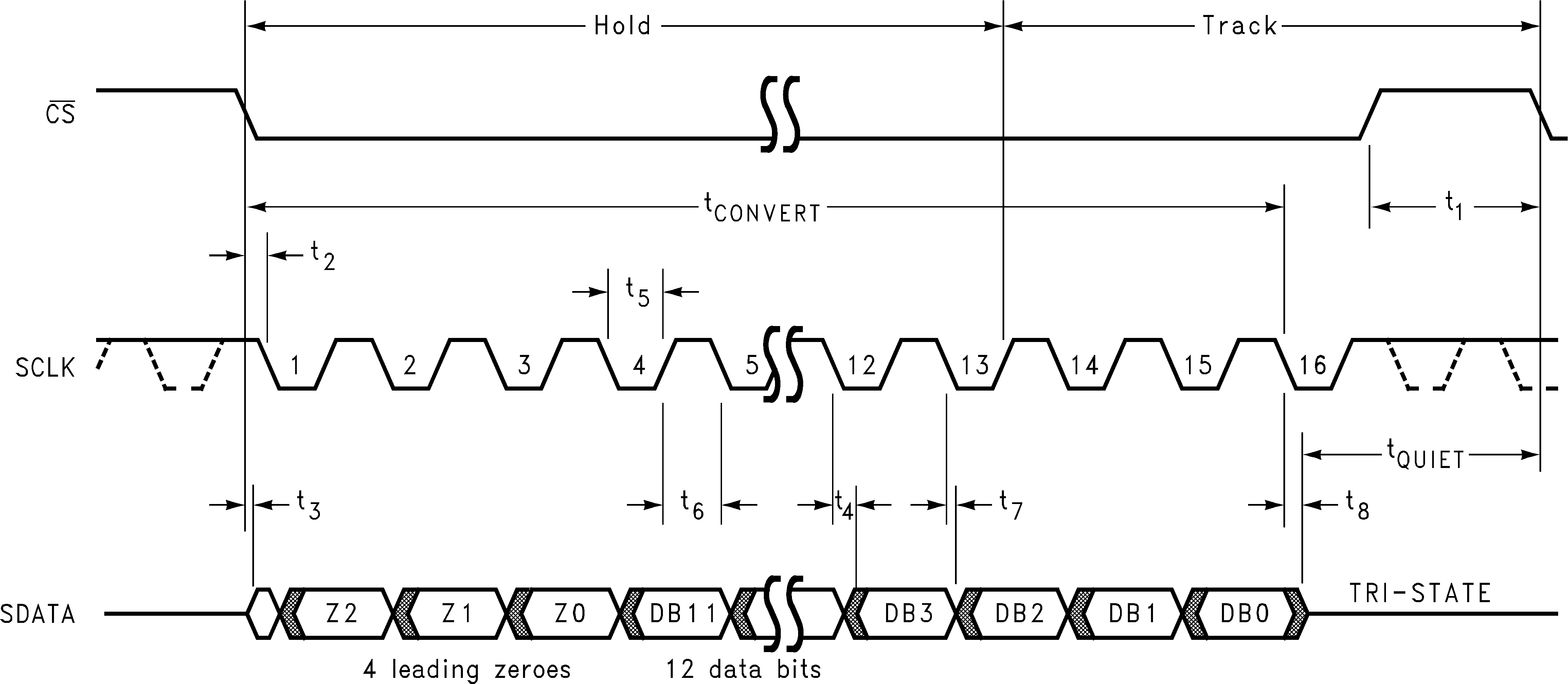 Figure 2. ADCS7476 Serial Interface Timing Diagram
 Figure 3. ADCS7477 Serial Interface Timing Diagram
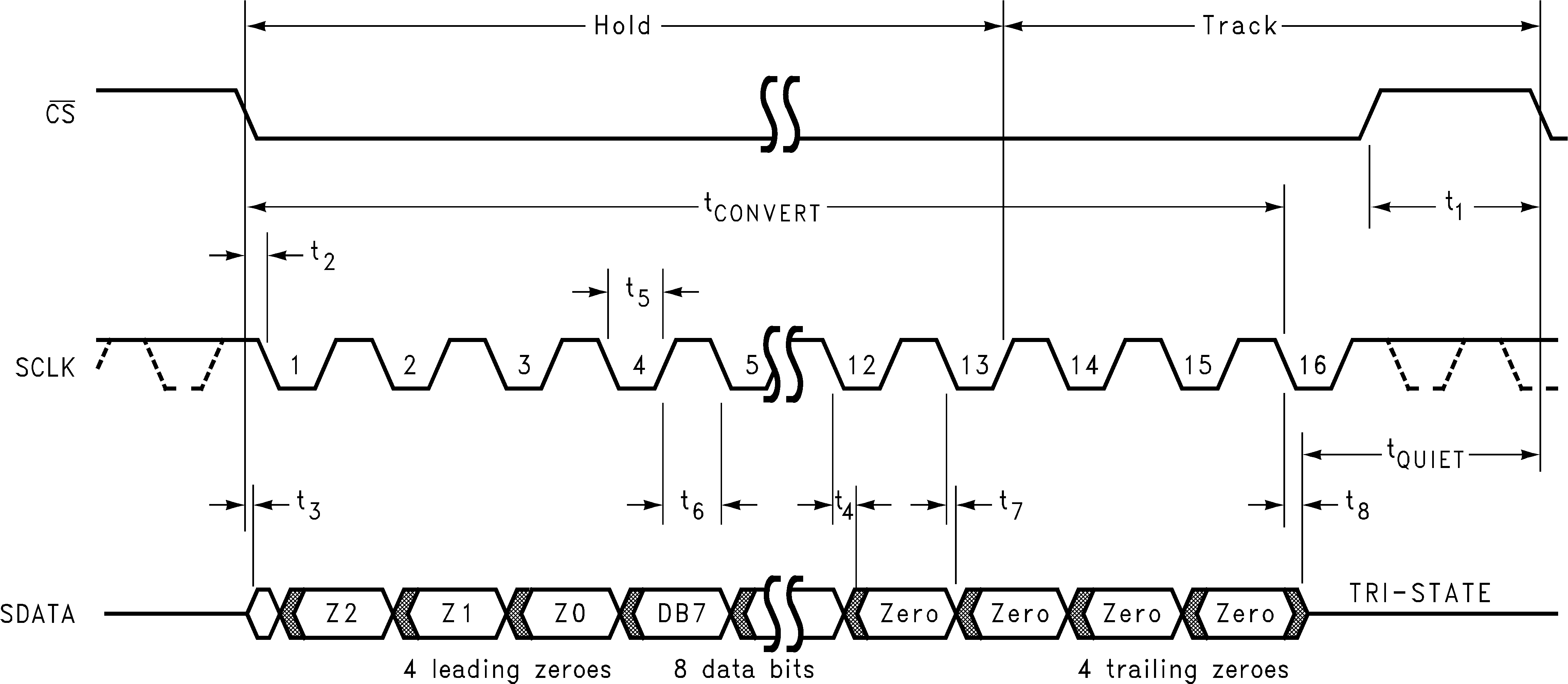 Figure 4. ADCS7478 Serial Interface Timing Diagram
6.9 Typical Characteristics
TA = 25°C, VDD = 3 V, fSAMPLE = 1 MSPS, fSCLK = 20 MHz, and fIN = 100 kHz (unless otherwise noted)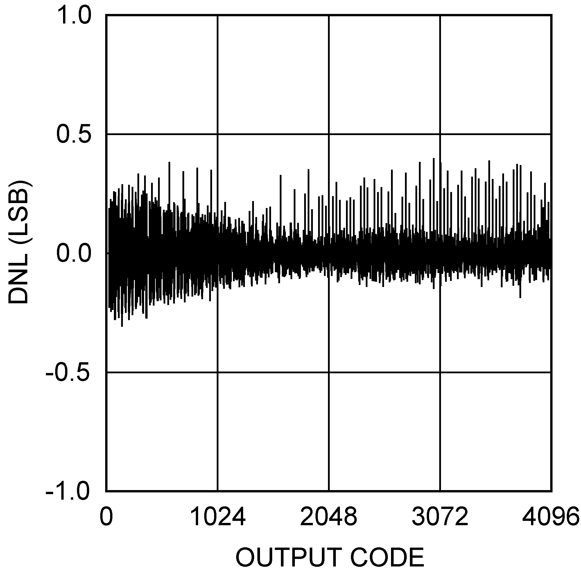 Figure 5. ADCS7476 DNL
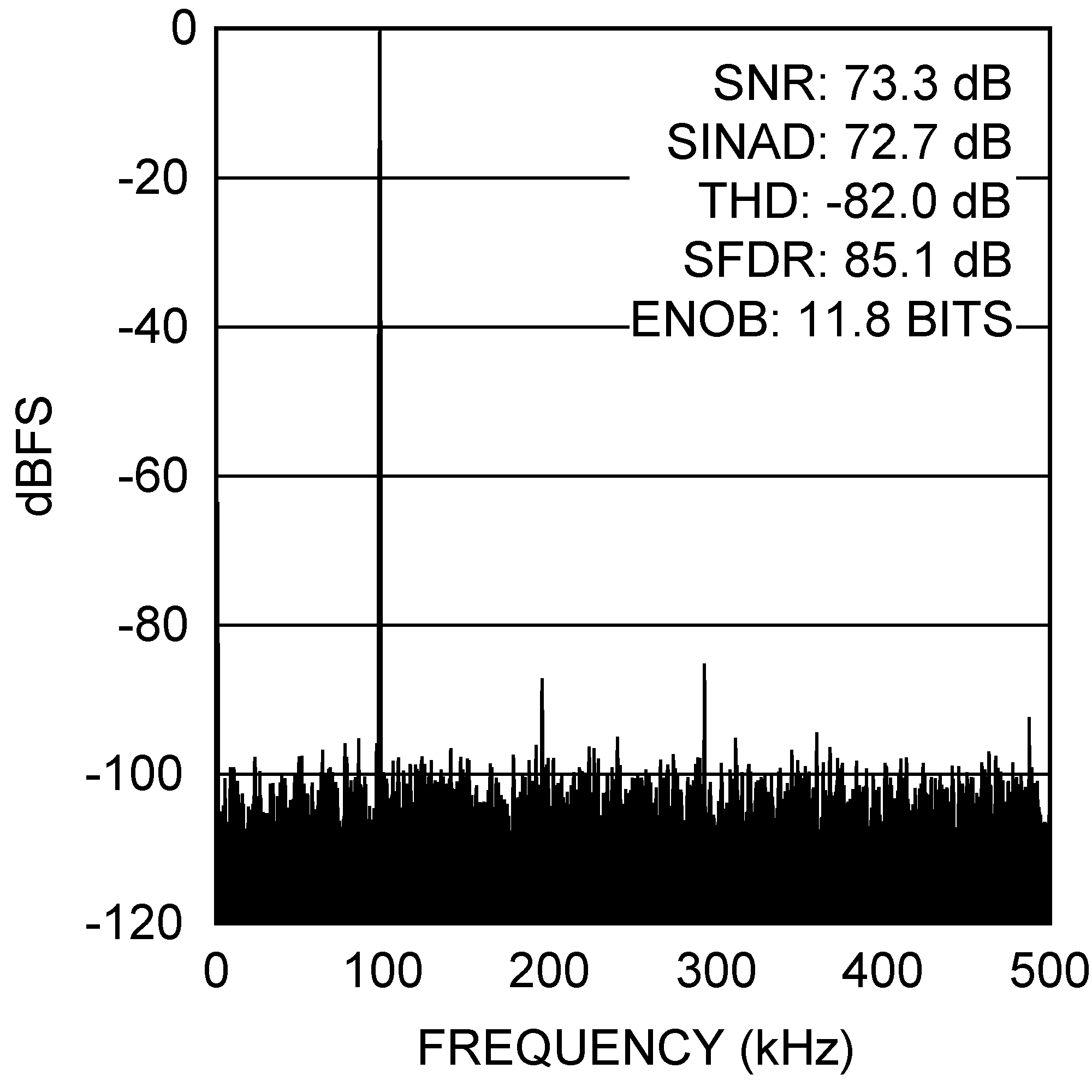 Figure 7. ADCS7476 Spectral Response at 100-kHz Input
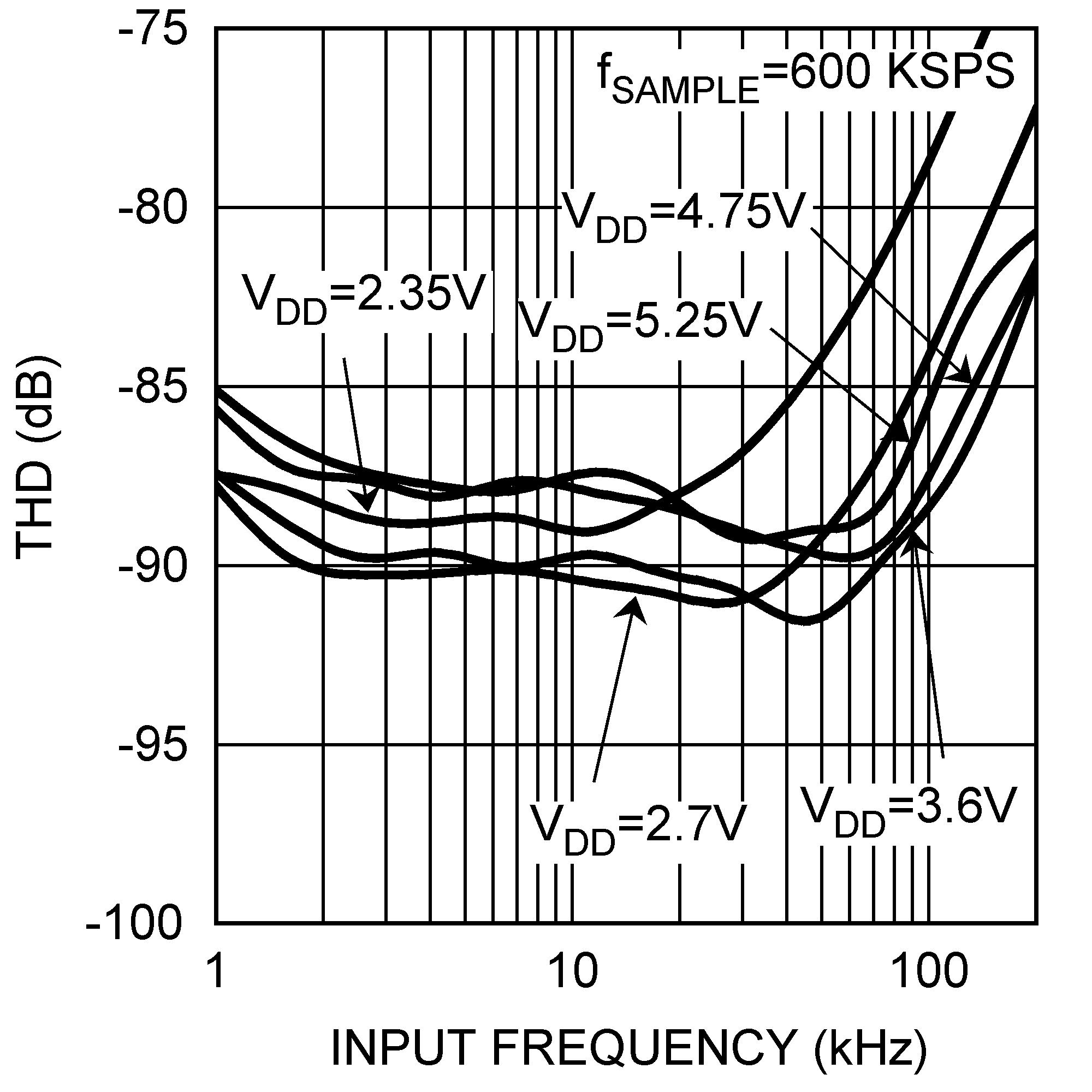 Figure 9. ADCS7476 THD vs Input Frequency, 600 KSPS
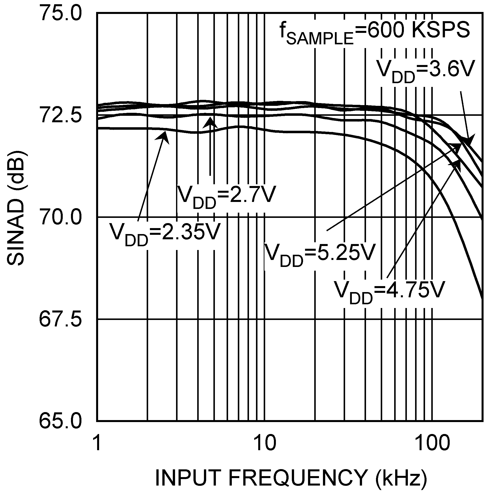 Figure 11. ADCS7476 SINAD vs Input Frequency, 600 KSPS
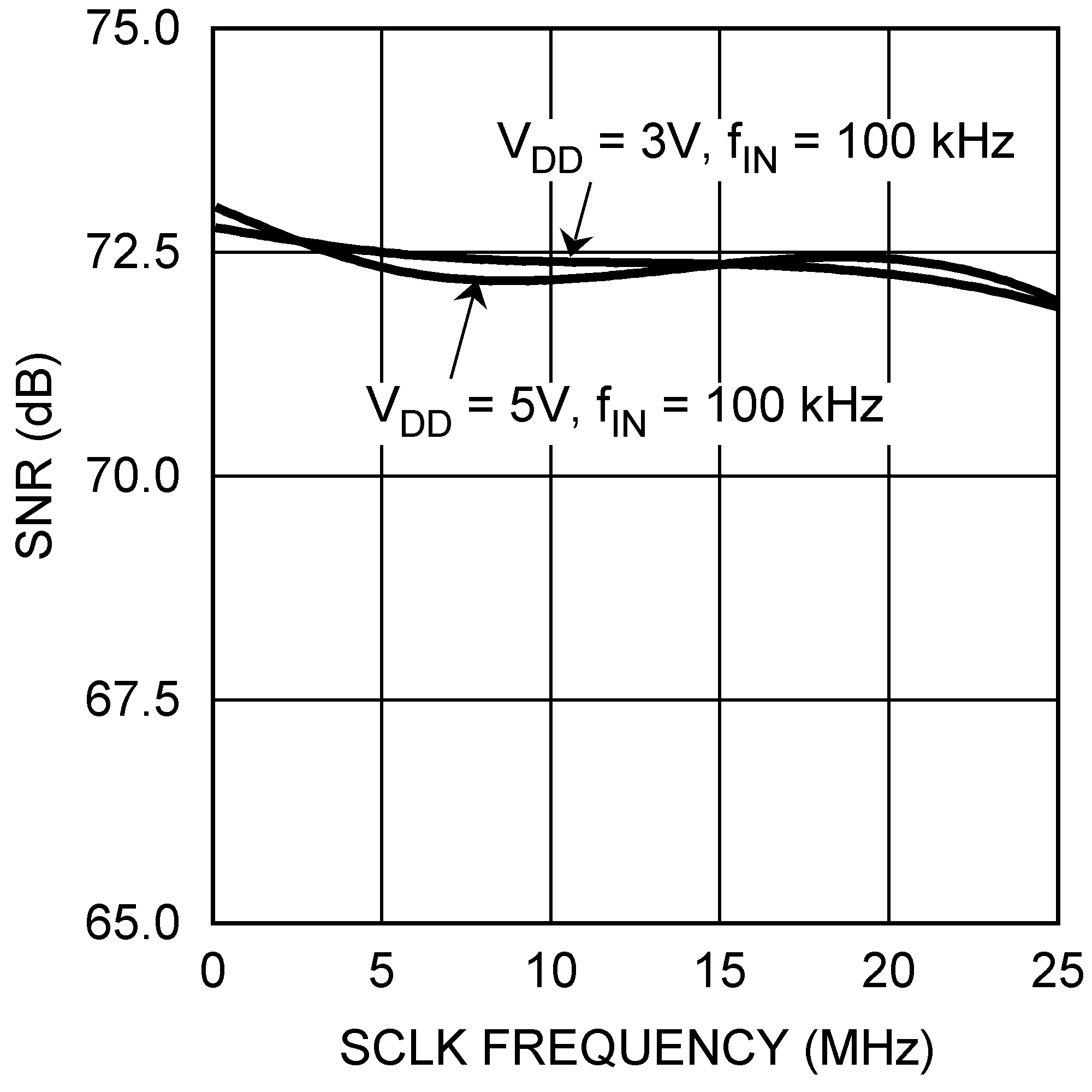 Figure 13. ADCS7476 SNR vs fSCLK
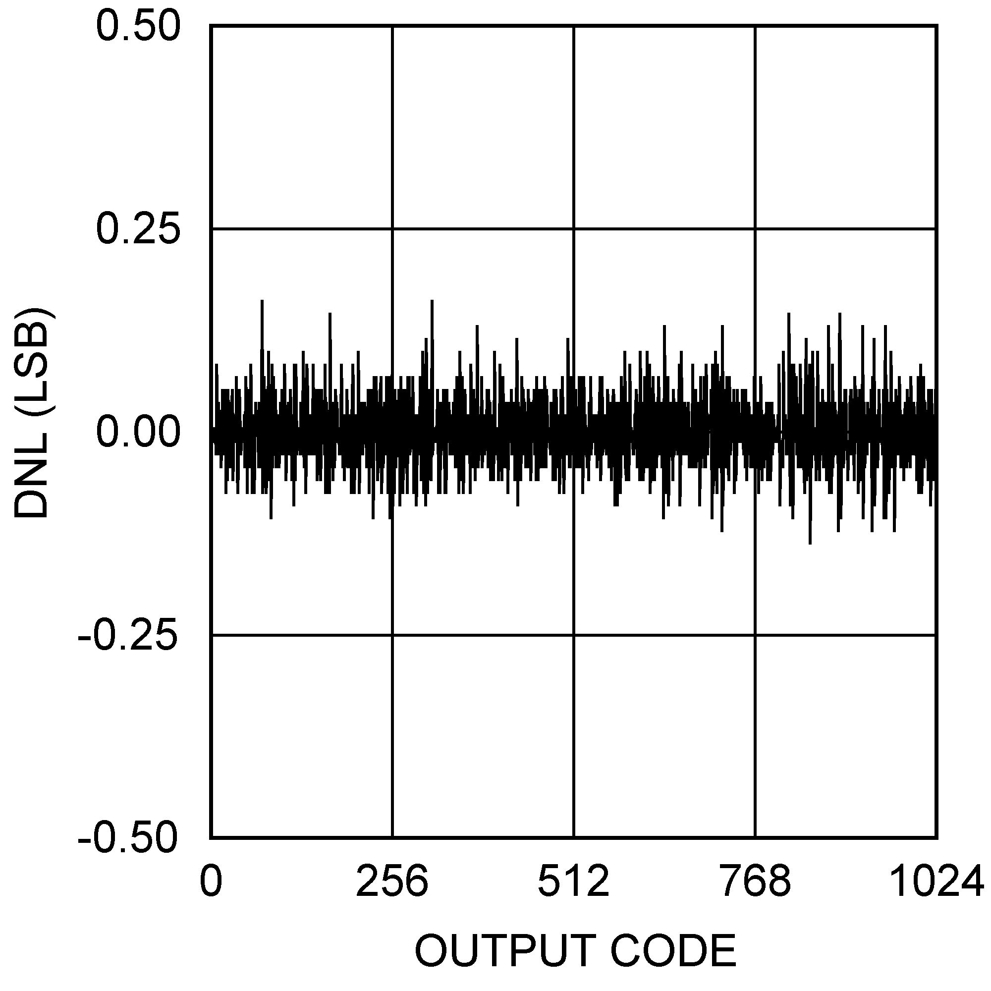 Figure 15. ADCS7477 DNL
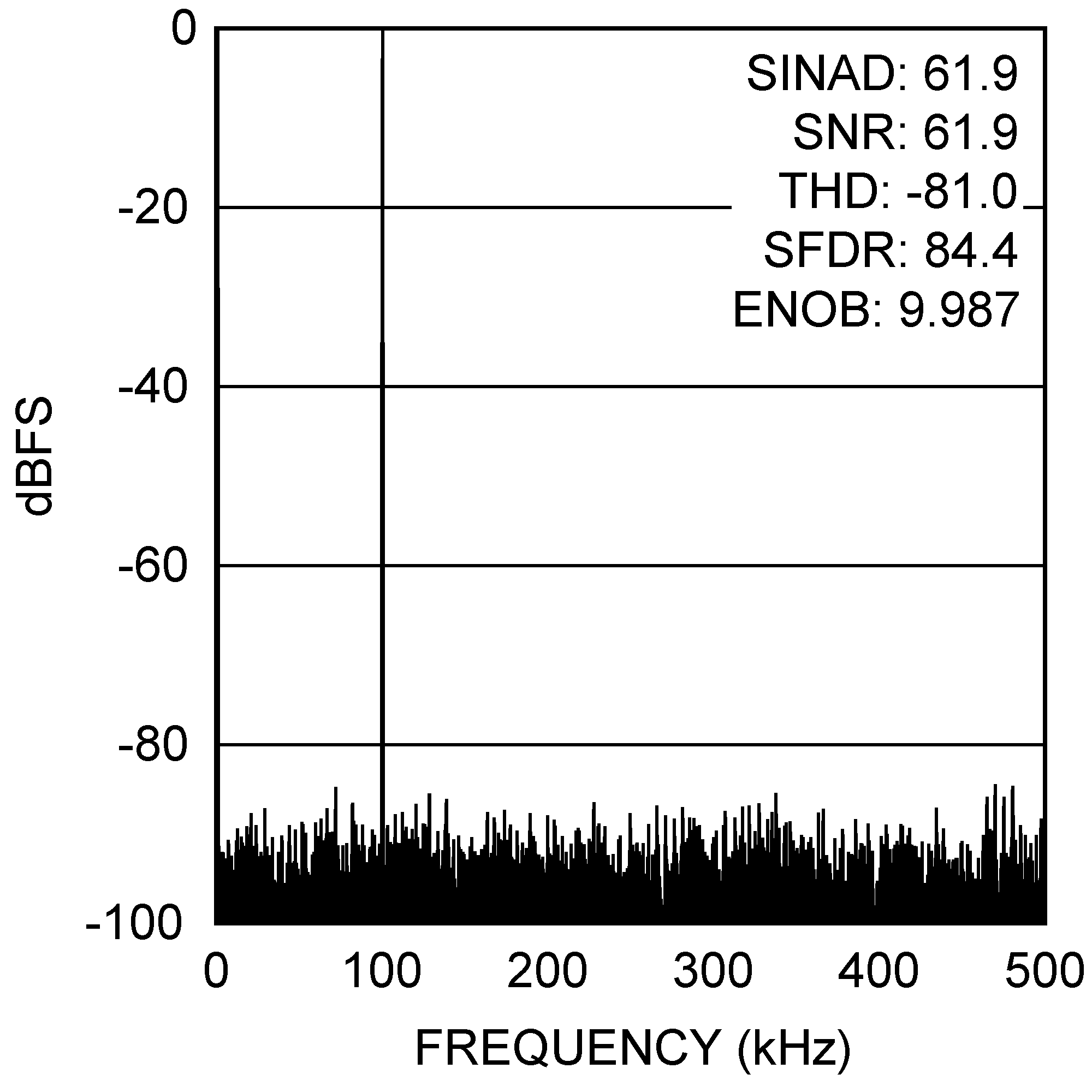 Figure 17. ADCS7477 Spectral Response at 100-kHz Input
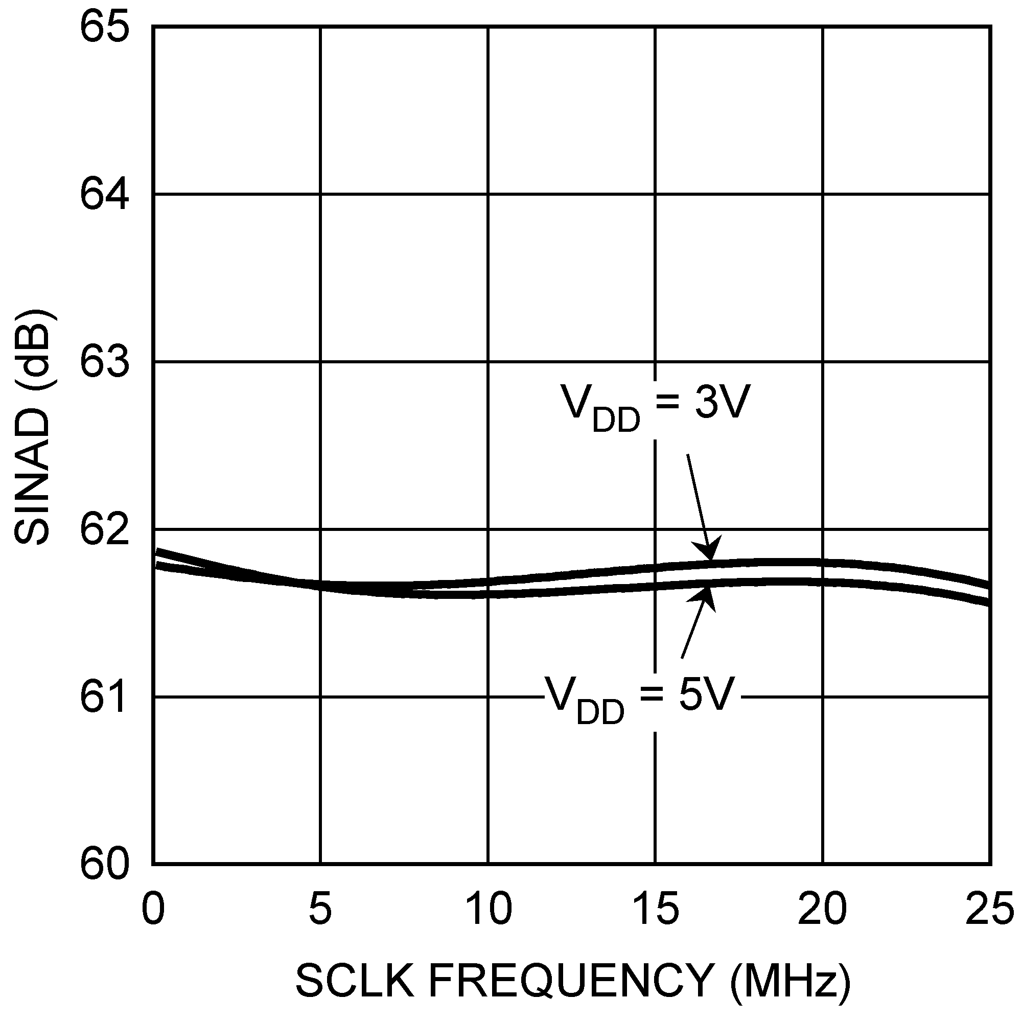 Figure 19. ADCS7477 SINAD vs fSCLK
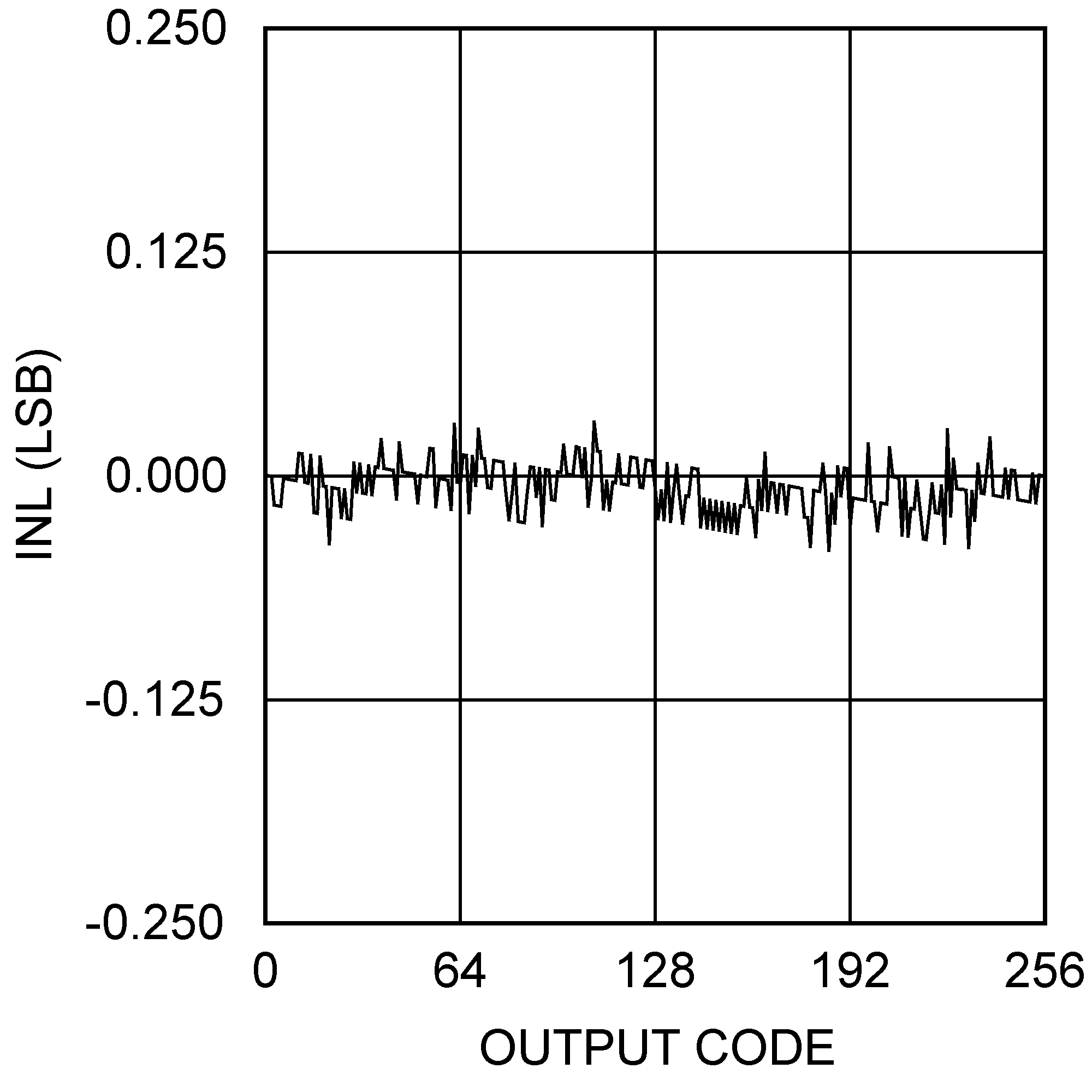 Figure 21. ADCS7478 INL
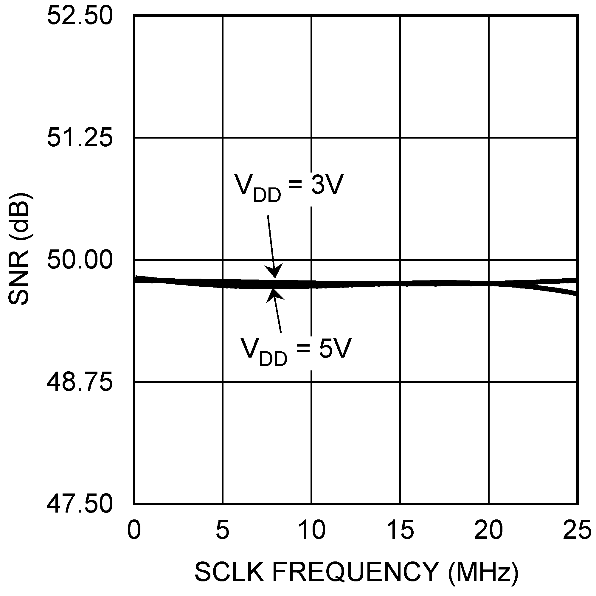 Figure 23. ADCS7478 SNR vs fSCLK
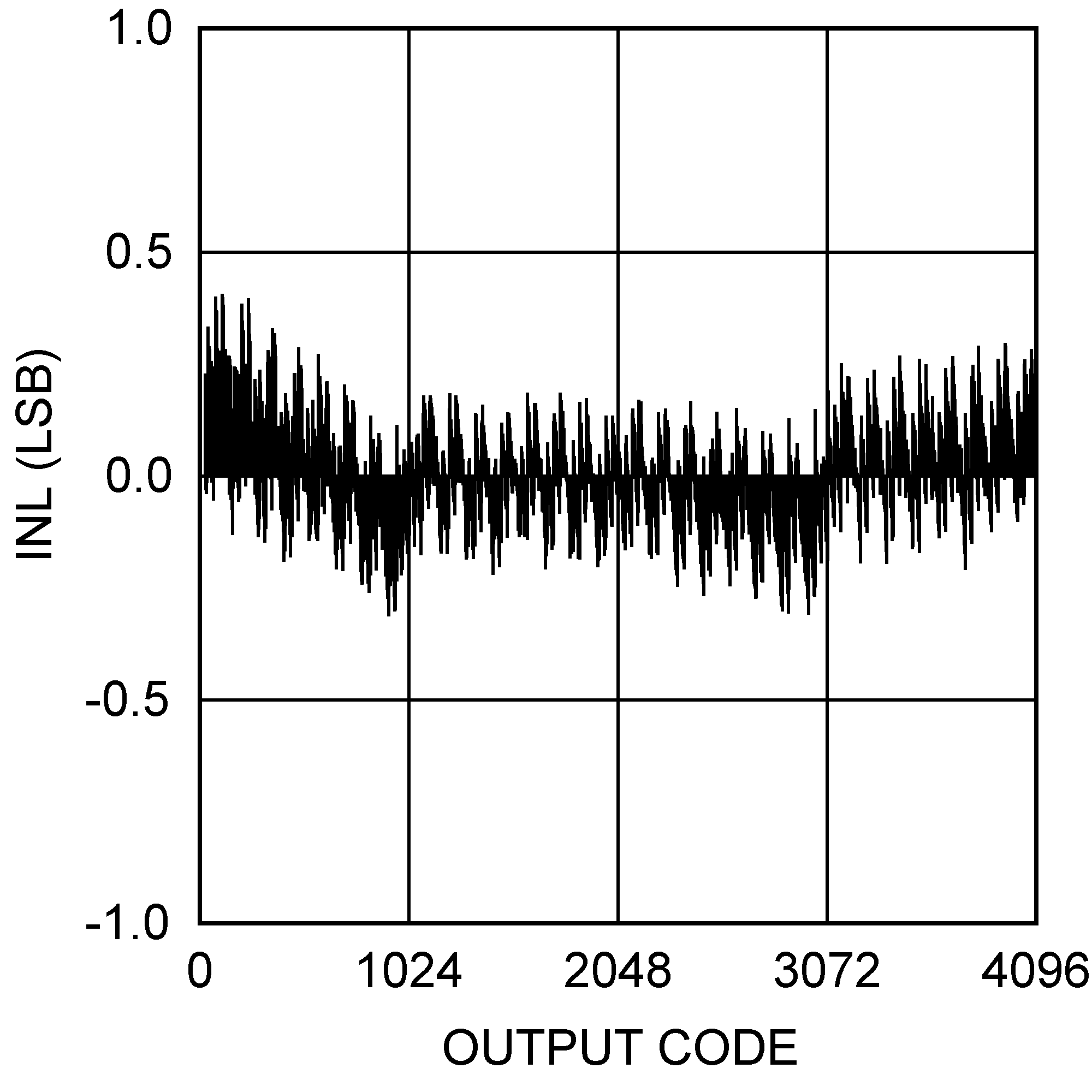 Figure 6. ADCS7476 INL
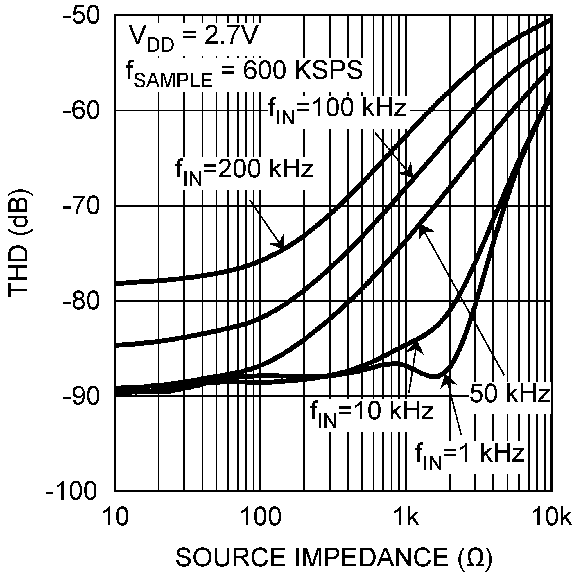 Figure 8. ADCS7476 THD vs Source Impedance
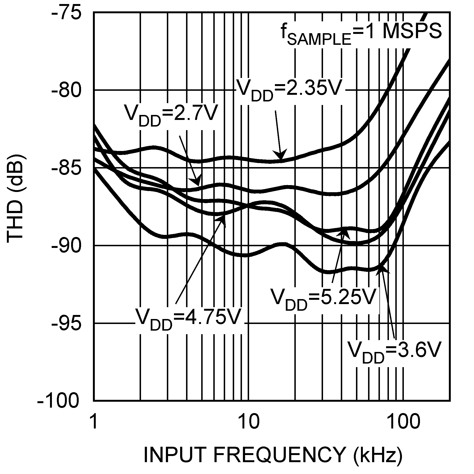 Figure 10. ADCS7476 THD vs Input Frequency, 1 MSPS
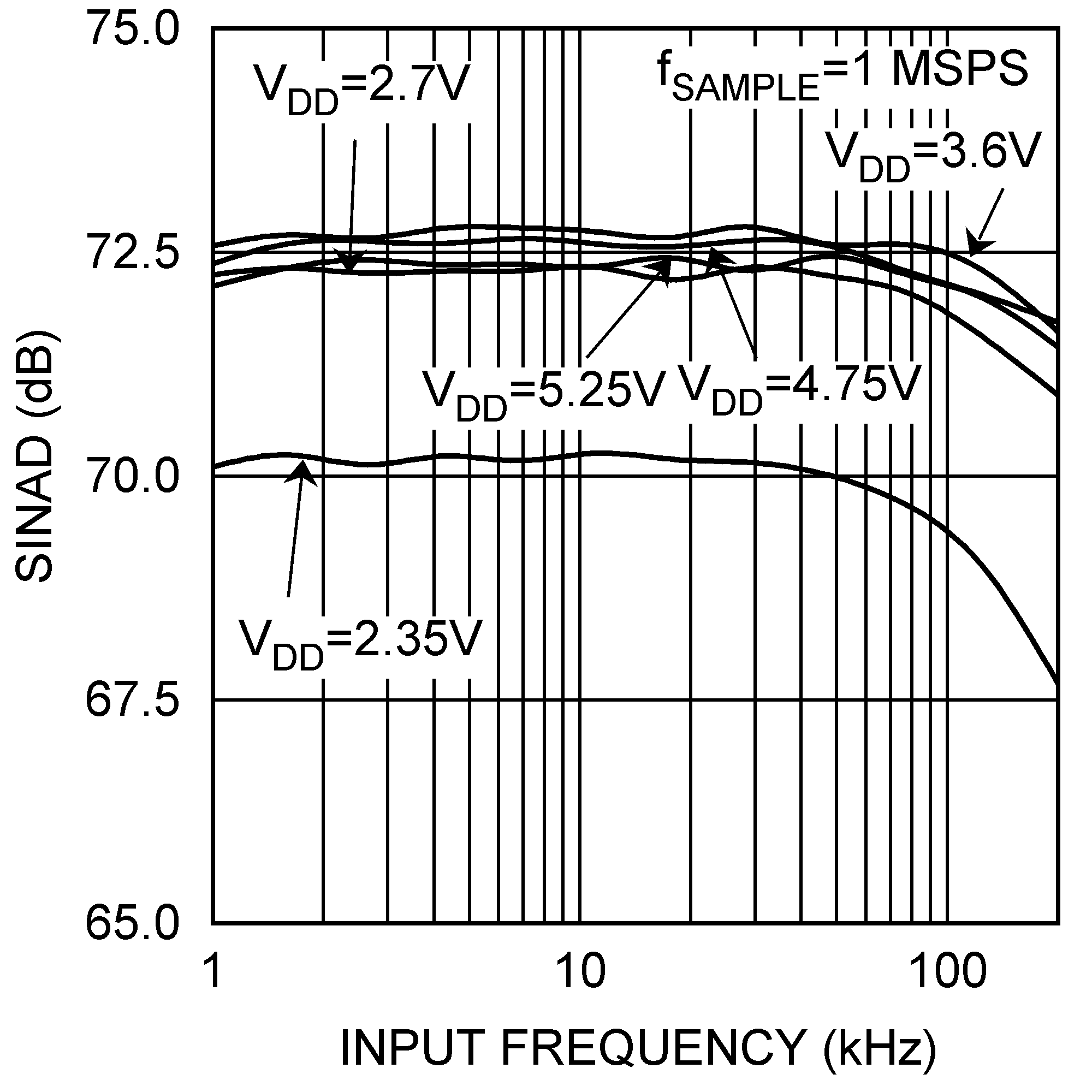 Figure 12. ADCS7476 SINAD vs Input Frequency, 1 MSPS
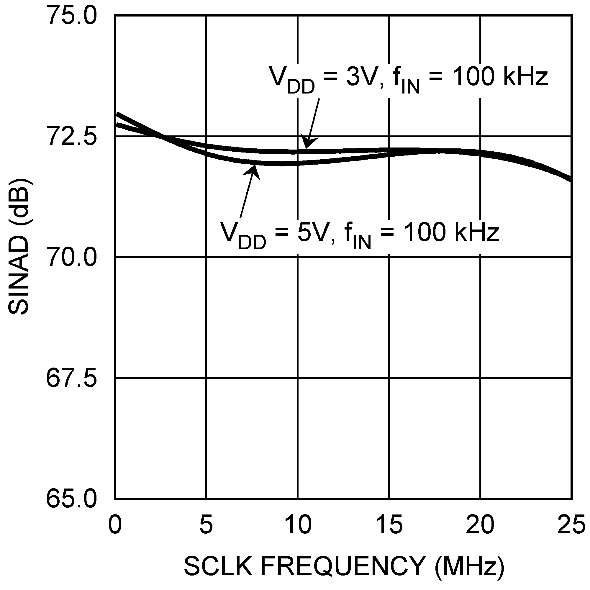 Figure 14. ADCS7476 SINAD vs fSCLK
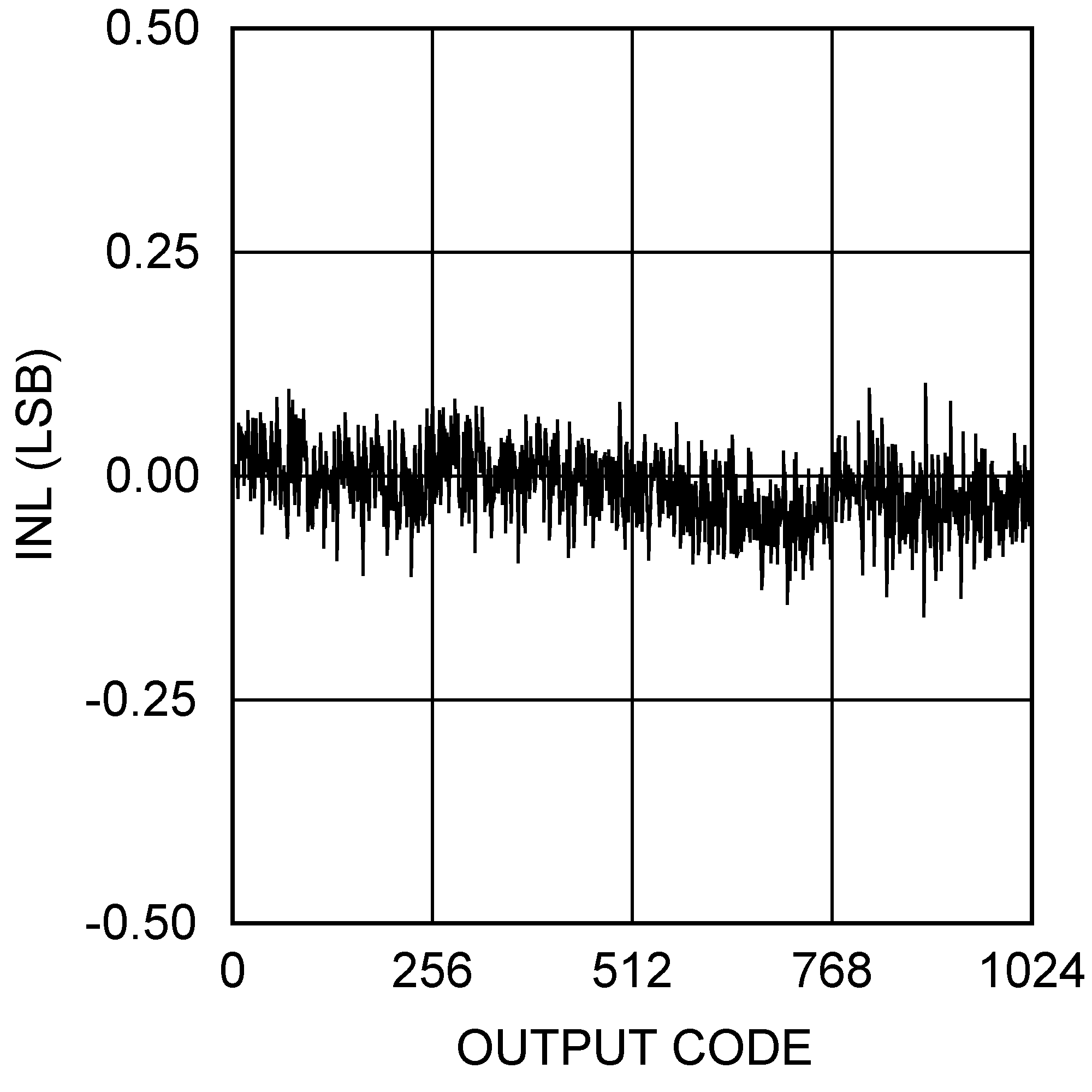 Figure 16. ADCS7477 INL
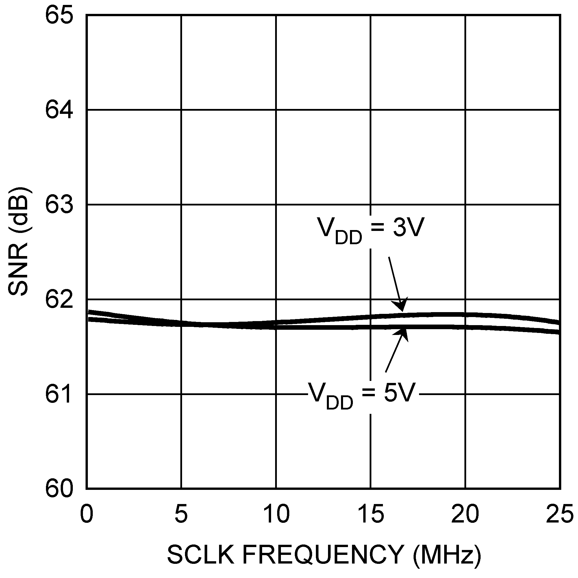 Figure 18. ADCS7477 SNR vs fSCLK
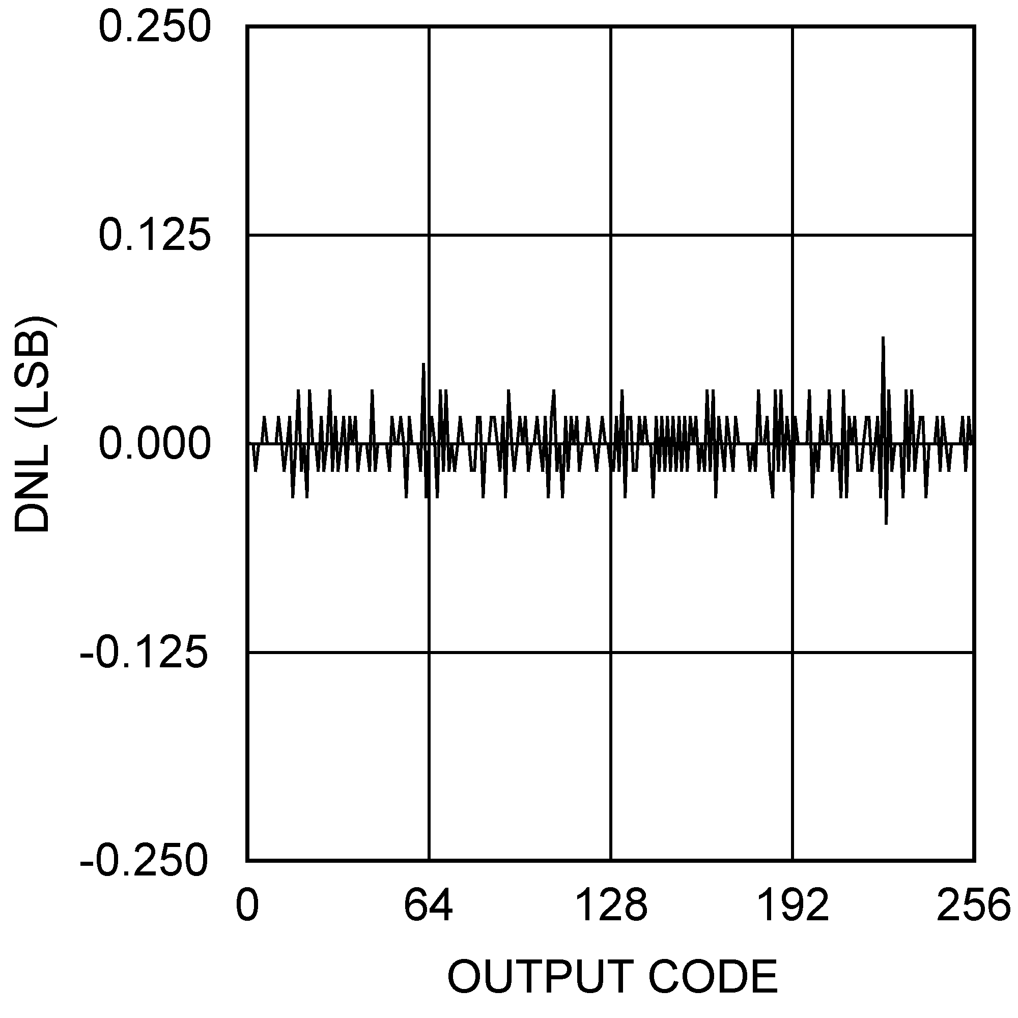 Figure 20. ADCS7478 DNL
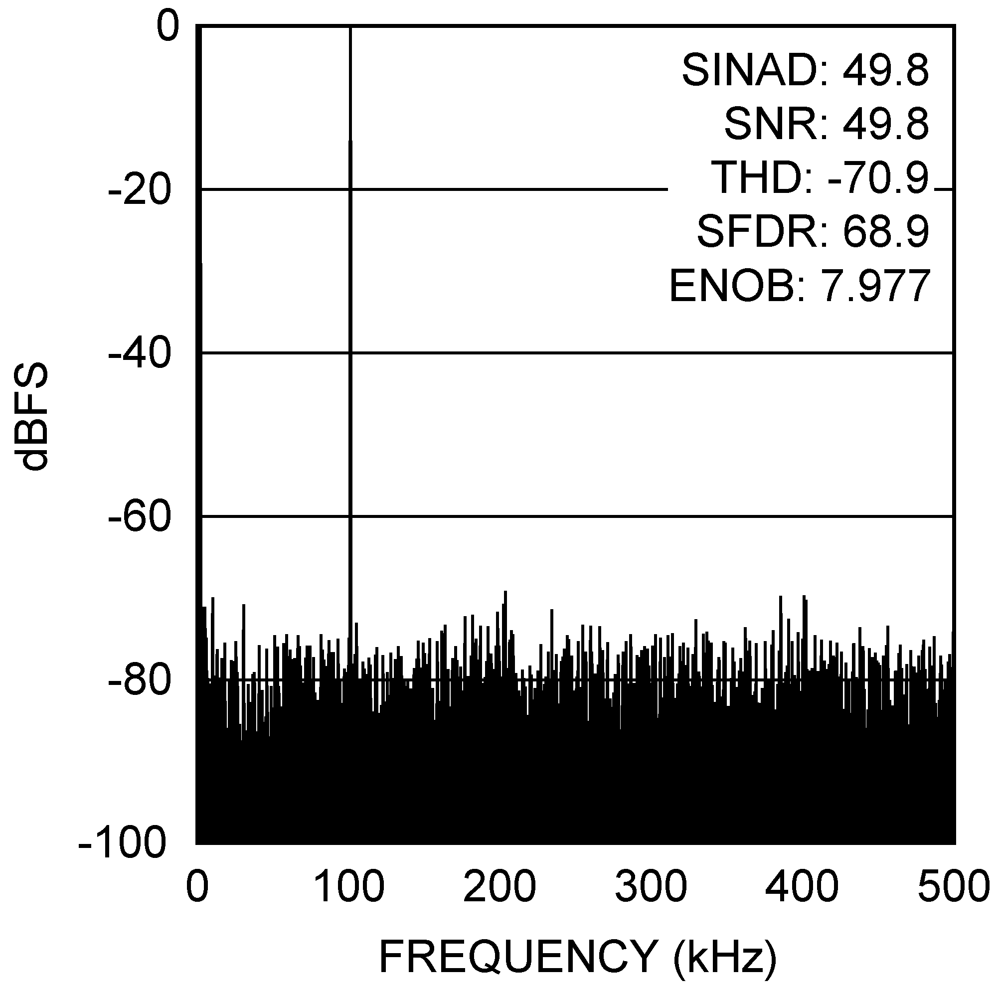 Figure 22. ADCS7478 Spectral Response at 100-kHz Input
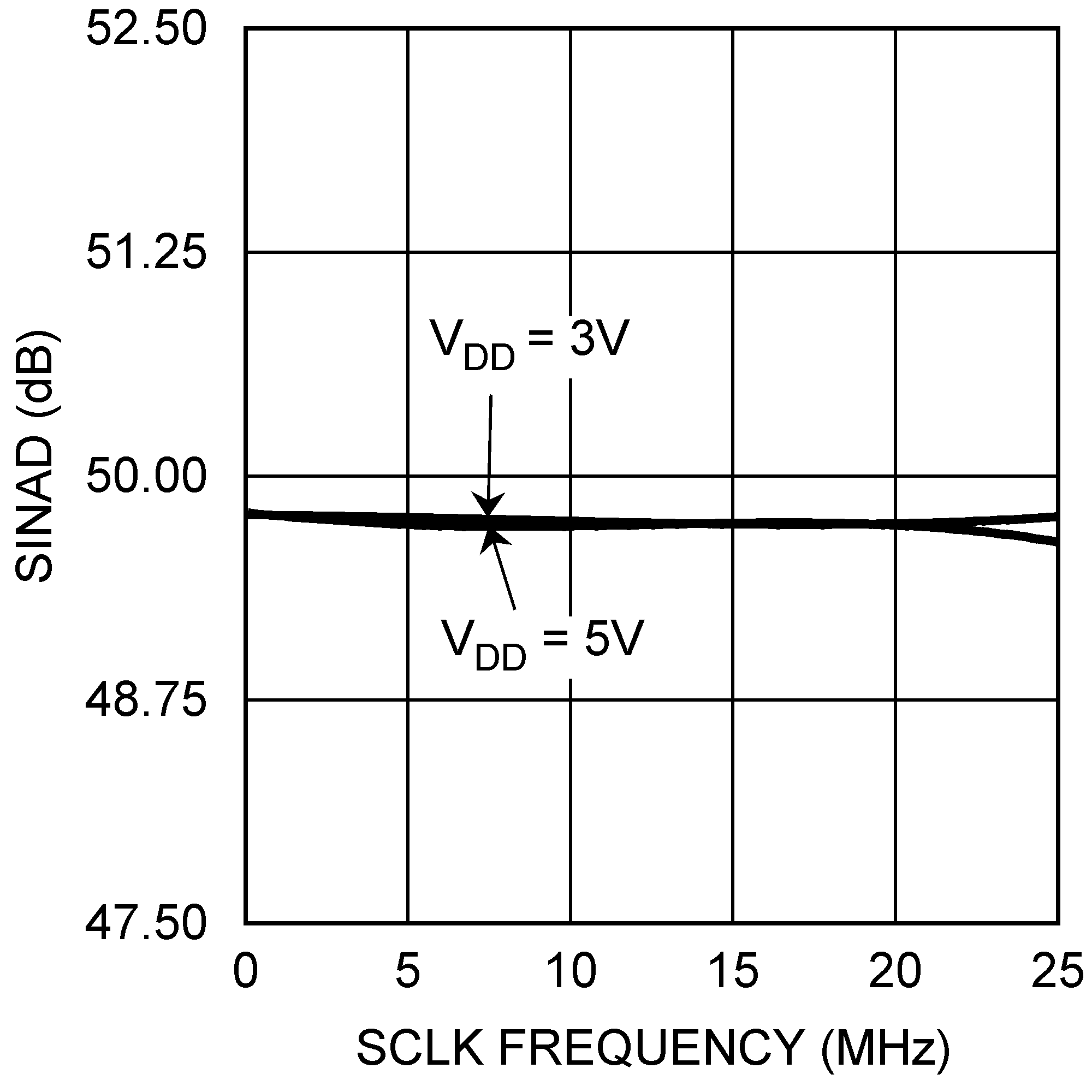 Figure 24. ADCS7478 SINAD vs fSCLK