JAJSA35G April 2003 – May 2016 ADCS7476 , ADCS7477 , ADCS7478
PRODUCTION DATA.
8 Application and Implementation
NOTE
Information in the following applications sections is not part of the TI component specification, and TI does not warrant its accuracy or completeness. TI’s customers are responsible for determining suitability of components for their purposes. Customers should validate and test their design implementation to confirm system functionality.
8.1 Application Information
A typical application of ADCS747x is shown in Figure 32. The combined analog and digital supplies are provided in this example by the TI LP2950 low-dropout voltage regulator, available in a variety of fixed and adjustable output voltages. The supply is bypassed with a capacitor network located close to the device. The three-wire interface is also shown connected to a microprocessor or DSP.
8.1.1 Analog Inputs
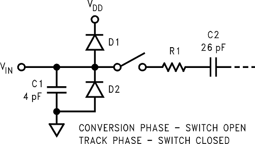
An equivalent circuit for the ADCS747x input channel is shown in Figure 31. The diodes D1 and D2 provide ESD protection for the analog inputs. At no time should an analog input exceed VDD + 300 mV or GND – 300 mV, as these ESD diodes begin conducting current into the substrate or supply line and affect ADC operation.
The capacitor C1 in Figure 31 typically has a value of 4 pF, and is mainly due to pin capacitance. The resistor R1 represents the ON resistance of the multiplexer and track or hold switch, and is typically 100 Ω. The capacitor C2 is the ADCS747x sampling capacitor, and is typically 26 pF.
The sampling nature of the analog input causes input current pulses that result in voltage spikes at the input. ADCS747x delivers best performance when driven by a low-impedance source to eliminate distortion caused by the charging of the sampling capacitance. In some applications where dynamic performance is critical, the input must be driven with a low output-impedance amplifier. In addition, when using ADCS747x to sample AC signals, a band-pass or low-pass filter reduces harmonics and noise and thus improve THD and SNR.
 Figure 31. Equivalent Input Circuit
8.1.2 Digital Inputs and Outputs
The ADCS747x digital inputs (SCLK and CS) are not limited by the same absolute maximum ratings as the analog inputs. The digital input pins are instead limited to 6.5 V with respect to GND, regardless of VDD, the supply voltage. This allows ADCS747x to be interfaced with a wide range of logic levels, independent of the supply voltage.
NOTE
Even though the digital inputs are tolerant of up to 6.5 V above GND, the digital outputs are only capable of driving VDD out.
In addition, the digital input pins are not prone to latch-up; SCLK and CS may be asserted before VDD without any risk.
8.2 Typical Application
The ADCS747x are monolithic CMOS 12-, 10-, and 8-bit ADCs that use the supply voltage as a reference, enabling the devices to operate with a full-scale input range of 0 to VDD. An example low-power application with the LMT87, which is a wide range ±0.3°C accurate temperature sensor, is shown in Figure 32.
 Figure 32. Typical Application Circuit
8.2.1 Design Requirements
A successful ADCS747x and LMT87 design is constrained by the following factors:
- VIN range must be 0 V to VDD where VDD can range from 2.7 V to 5.25 V.
8.2.2 Detailed Design Procedure
Designing for an accurate measurement requires careful attention to the timing requirements for the ADCS747x parts.
Because the ADC747x parts use the supply voltage as a reference, ensuring that the supply voltage is settled to its final level before exiting the shutdown mode and beginning a conversion is important. After the supply voltage has settled, the CS is brought to a low level (ideally 0 V) to start a conversion.
Ensuring that any noise on the power supply is less than ½ LSB in amplitude is also important. The supply voltage must be regarded as a precise voltage reference.
After the CS has been brought low, the user must wait for one complete conversion cycle (approximately 1 μs) for meaningful data. The dummy conversion cycle is the start-up time of the ADCS747x. The ADCS747x digital output can then be correlated to the LMT87 output level to get an accurate temperature reading. At VDD = 3.3 V,
1 LSB of ADCS7476 is 0.805 mV.
8.2.3 Application Curves
 Figure 33. ADCS7476/77 Ideal Transfer Characteristic
 Figure 34. ADCS7478 Ideal Transfer Characteristic