SBAS741B October 2015 – April 2020 ADS1018-Q1
PRODUCTION DATA.
- 1 Features
- 2 Applications
- 3 Description
- 4 Revision History
- 5 Device Comparison Table
- 6 Pin Configuration and Functions
- 7 Specifications
- 8 Detailed Description
- 9 Application and Implementation
- 10Power Supply Recommendations
- 11Layout
- 12Device and Documentation Support
- 13Mechanical, Packaging, and Orderable Information
9.2.2 Detailed Design Procedure
The biasing resistors (RPU and RPD) serve two purposes. The first purpose is to set the common-mode voltage of the thermocouple to within the specified voltage range of the device. The second purpose is to offer a weak pullup and pulldown to detect an open thermocouple lead. When one of the thermocouple leads fails open, the positive input is pulled to VDD and the negative input is pulled to GND. The ADC consequently reads a full-scale value that is outside the normal measurement range of the thermocouple voltage to indicate this failure condition. When choosing the values of the biasing resistors, take care so that the biasing current does not degrade measurement accuracy. The biasing current flows through the thermocouple and can cause self-heating and additional voltage drops across the thermocouple leads. Typical values for the biasing resistors range from 1 MΩ to 50 MΩ.
Although the device digital filter attenuates high-frequency components of noise, provide a first-order, passive RC filter at the inputs to further improve performance. The differential RC filter formed by RDIFFA, RDIFFB, and the differential capacitor CDIFF offers a cutoff frequency that is calculated using Equation 3. While the digital filter of the ADS1018-Q1 strongly attenuates high-frequency components of noise, provide a first-order, passive RC filter to further suppress high-frequency noise and avoid aliasing. Care must be taken when choosing the filter resistor values because the input currents flowing into and out of the device cause a voltage drop across the resistors. This voltage drop shows up as an additional offset error at the ADC inputs. Limit the filter resistor values to below 1 kΩ for best performance.
Two common-mode filter capacitors (CCMA and CCMB) are also added to offer attenuation of high-frequency, common-mode noise components. Differential capacitor CDIFF must be at least an order of magnitude (10x) larger than these common-mode capacitors because mismatches in the common-mode capacitors can convert common-mode noise into differential noise.
The highest measurement resolution is achieved when the largest potential input signal is slightly lower than the FSR of the ADC. From the design requirement, the maximum thermocouple voltage (VTC) occurs at a thermocouple temperature (TTC) of 1250°C. At this temperature, VTC = 50.644 mV, as defined in the tables published by the National Institute of Standards and Technology (NIST) using a cold-junction temperature (TCJ) of 0°C. A thermocouple produces an output voltage that is proportional to the temperature difference between the thermocouple tip and the cold junction. If the cold junction is at a temperature below 0°C, the thermocouple produces a voltage larger than 50.644 mV. The isothermal block area is constrained by the operating temperature range of the device. Therefore, the isothermal block temperature is limited to –40°C. A K-type thermocouple at TTC = 1250°C produces an output voltage of VTC = 50.644 mV – (–1.527 mV) = 52.171 mV when referenced to a cold-junction temperature of TCJ = –40°C. The device offers a full-scale range of ±0.256 V and that is what is used in this application example.
The device integrates a high-precision temperature sensor that can be used to measure the temperature of the cold junction. The temperature sensor mode is enabled by setting bit TS_MODE = 1 in the Config register. The accuracy of the overall temperature sensor depends on how accurately the ADS1018-Q1 can measure the cold junction, and hence, careful component placement and PCB layout considerations must be employed for designing an accurate thermocouple system. The ADS1118 evaluation module provides a good starting point and offers an example to achieve good cold-junction compensation performance. The ADS1118 evaluation module uses the same schematic as shown in Figure 23, except with only one thermocouple channel connected. Refer to the Precision Thermocouple Measurement With the ADS1118 application note for details on how to optimize your component placement and layout to achieve good cold-junction compensation performance.
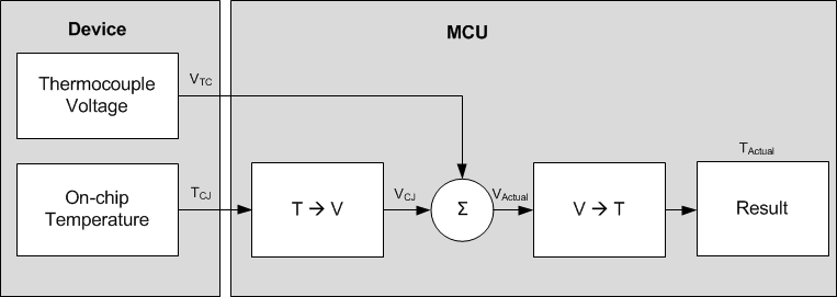
The calculation procedure to achieve cold-junction compensation can be done in several ways. A typical way is to interleave readings between the thermocouple inputs and the temperature sensor. That is, acquire one on-chip temperature result, TCJ, for every thermocouple ADC voltage measured, VTC. To account for the cold junction, first convert the temperature sensor reading within the ADS1018-Q1 to a voltage (VCJ) that is proportional to the thermocouple currently being used. This process is generally accomplished by performing a reverse lookup on the table used for the thermocouple voltage-to-temperature conversion. Adding these two voltages yields the thermocouple-compensated voltage (VActual), where VActual = VCJ + VTC. VActual is then converted to a temperature (TActual) using the same NIST lookup table. A block diagram showing this process is given in Figure 24. Refer to the Precision Thermocouple Measurement With the ADS1118 application note for a detailed explanation of this method.
 Figure 24. Software-Flow Block Diagram
 Figure 25 and Figure 26 show the expected measurement results. A system offset calibration is performed at TTC = 25°C that equates to VTC = 0 V when TCJ = 25°C. The dashed blue lines in Figure 25 show the maximum error guard band due to ADC gain and nonlinearity error. The dashed blue lines in Figure 26 show the corresponding temperature measurement error guard band calculated from the data in Figure 25 using the NIST tables. The dashed red lines in Figure 26 include the guard band for the temperature sensor inaccuracy (±1°C), in addition to the device gain and nonlinearity error. Note that the results in Figure 25 and Figure 26 do not account for the thermocouple inaccuracy that must also be considered while designing a thermocouple measurement system.