JAJSDU5A August 2017 – February 2020 ADS114S06B , ADS114S08B
PRODUCTION DATA.
- 1 特長
- 2 アプリケーション
- 3 概要
- 4 改訂履歴
- 5 Device Comparison Table
- 6 Pin Configuration and Functions
- 7 Specifications
- 8 Parameter Measurement Information
-
9 Detailed Description
- 9.1 Overview
- 9.2 Functional Block Diagram
- 9.3
Feature Description
- 9.3.1 Multiplexer
- 9.3.2 Low-Noise Programmable Gain Amplifier
- 9.3.3 Voltage Reference
- 9.3.4 Clock Source
- 9.3.5 Delta-Sigma Modulator
- 9.3.6 Digital Filter
- 9.3.7 Excitation Current Sources (IDACs)
- 9.3.8 Bias Voltage Generation
- 9.3.9 System Monitor
- 9.3.10 Status Register
- 9.3.11 General-Purpose Inputs and Outputs (GPIOs)
- 9.3.12 Calibration
- 9.4 Device Functional Modes
- 9.5 Programming
- 9.6
Register Map
- 9.6.1 Configuration Registers
- 9.6.2
Register Descriptions
- 9.6.2.1 Device ID Register (address = 00h) [reset = xxh]
- 9.6.2.2 Device Status Register (address = 01h) [reset = 80h]
- 9.6.2.3 Input Multiplexer Register (address = 02h) [reset = 01h]
- 9.6.2.4 Gain Setting Register (address = 03h) [reset = 00h]
- 9.6.2.5 Data Rate Register (address = 04h) [reset = 14h]
- 9.6.2.6 Reference Control Register (address = 05h) [reset = 10h]
- 9.6.2.7 Excitation Current Register 1 (address = 06h) [reset = 00h]
- 9.6.2.8 Excitation Current Register 2 (address = 07h) [reset = FFh]
- 9.6.2.9 Sensor Biasing Register (address = 08h) [reset = 00h]
- 9.6.2.10 System Control Register (address = 09h) [reset = 10h]
- 9.6.2.11 Reserved Register (address = 0Ah) [reset = 00h]
- 9.6.2.12 Offset Calibration Register 1 (address = 0Bh) [reset = 00h]
- 9.6.2.13 Offset Calibration Register 2 (address = 0Ch) [reset = 00h]
- 9.6.2.14 Reserved Register (address = 0Dh) [reset = 00h]
- 9.6.2.15 Gain Calibration Register 1 (address = 0Eh) [reset = 00h]
- 9.6.2.16 Gain Calibration Register 2 (address = 0Fh) [reset = 40h]
- 9.6.2.17 GPIO Data Register (address = 10h) [reset = 00h]
- 9.6.2.18 GPIO Configuration Register (address = 11h) [reset = 00h]
- 10Application and Implementation
- 11Power Supply Recommendations
- 12Layout
- 13デバイスおよびドキュメントのサポート
- 14メカニカル、パッケージ、および注文情報
パッケージ・オプション
デバイスごとのパッケージ図は、PDF版データシートをご参照ください。
メカニカル・データ(パッケージ|ピン)
- RHB|32
- PBS|32
サーマルパッド・メカニカル・データ
- PBS|32
発注情報
9.3.6.3 Note on Conversion Time
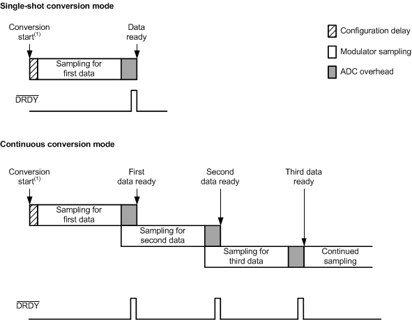
Each data period consists of time required for the modulator to sample the analog inputs. However, there is additional time required before the samples become an ADC conversion result.
When a new conversion is started, there is a configuration delay time of 14 · tMOD (where tMOD = 16 · tCLK) that is added before the conversion starts. This delay allows for additional settling time for external RC filters on the analog inputs and for the antialiasing filter after the PGA. The configuration delay occurs at the start of a new conversion after a START command is sent, the START/SYNC pin is taken high, or a WREG command is sent to change any configuration register from address 03h to 07h (as described in the WREG section).
Also, overhead time is needed to convert the modulator samples into an ADC conversion result. This overhead time includes any necessary offset or gain compensation after the digital filter accumulates a data result. The first conversion when the device is in continuous conversion mode (just as in single-shot conversion mode) includes the configuration delay, the modulator sampling time, and the overhead time. The second and subsequent conversions are the normal data period (period as given by the inverse of the data rate).
Figure 62 shows the time sequence for the ADC in both continuous conversion and single-shot conversion modes.
