JAJSP40A
March 2022 – October 2022
ADS117L11
PRODUCTION DATA
1
特長
2
アプリケーション
3
概要
4
Revision History
5
Pin Configuration and Functions
6
Specifications
6.1
Absolute Maximum Ratings
6.2
ESD Ratings
6.3
Recommended Operating Conditions
6.4
Thermal Information
6.5
Electrical Characteristics
6.6
Timing Requirements (1.65 V ≤ IOVDD ≤ 2 V)
6.7
Switching Characteristics (1.65 V ≤ IOVDD ≤ 2 V)
6.8
Timing Requirements (2 V < IOVDD ≤ 5.5 V)
6.9
Switching Characteristics (2 V < IOVDD ≤ 5.5 V)
6.10
Timing Diagrams
6.11
Typical Characteristics
7
Parameter Measurement Information
7.1
Offset Error Measurement
7.2
Offset Drift Measurement
7.3
Gain Error Measurement
7.4
Gain Drift Measurement
7.5
NMRR Measurement
7.6
CMRR Measurement
7.7
PSRR Measurement
7.8
INL Error Measurement
7.9
THD Measurement
7.10
SFDR Measurement
7.11
Noise Performance
8
Detailed Description
8.1
Overview
8.2
Functional Block Diagram
8.3
Feature Description
8.3.1
Analog Input (AINP, AINN)
8.3.1.1
Input Range
8.3.2
Reference Voltage (REFP, REFN)
8.3.2.1
Reference Voltage Range
8.3.3
Clock Operation
8.3.3.1
Internal Oscillator
8.3.3.2
External Clock
8.3.4
Modulator
8.3.5
Digital Filter
8.3.5.1
Wideband Filter
8.3.5.2
Low-Latency Filter (Sinc)
8.3.5.2.1
Sinc4 Filter
8.3.5.2.2
Sinc4 + Sinc1 Filter
8.3.5.2.3
Sinc3 Filter
8.3.5.2.4
Sinc3 + Sinc1 Filter
8.3.6
Power Supplies
8.3.6.1
AVDD1 and AVSS
8.3.6.2
AVDD2
8.3.6.3
IOVDD
8.3.6.4
Power-On Reset (POR)
8.3.6.5
CAPA and CAPD
8.3.7
VCM Output Voltage
8.4
Device Functional Modes
8.4.1
Power-Scalable Speed Modes
8.4.2
Idle Mode
8.4.3
Standby Mode
8.4.4
Power-Down Mode
8.4.5
Reset
8.4.5.1
RESET Pin
8.4.5.2
Reset by SPI Register Write
8.4.5.3
Reset by SPI Input Pattern
8.4.6
Synchronization
8.4.6.1
Synchronized Control Mode
8.4.6.2
Start/Stop Control Mode
8.4.6.3
One-Shot Control Mode
8.4.7
Conversion-Start Delay Time
8.4.8
Calibration
8.4.8.1
OFFSET2, OFFSET1, OFFSET0 Calibration Registers (Addresses 9h, Ah, Bh)
8.4.8.2
GAIN2, GAIN1, GAIN0 Calibration Registers (Addresses 0Ch, 0Dh, 0Eh)
8.4.8.3
Calibration Procedure
8.5
Programming
8.5.1
Serial Interface (SPI)
8.5.1.1
Chip Select (CS)
8.5.1.2
Serial Clock (SCLK)
8.5.1.3
Serial Data Input (SDI)
8.5.1.4
Serial Data Output/Data Ready (SDO/DRDY)
8.5.2
SPI Frame
8.5.3
SPI CRC
8.5.4
Register Map CRC
8.5.5
Full-Duplex Operation
8.5.6
Device Commands
8.5.6.1
No-Operation
8.5.6.2
Read Register Command
8.5.6.3
Write Register Command
8.5.7
Read Conversion Data
8.5.7.1
Conversion Data
8.5.7.2
Data Ready
8.5.7.2.1
DRDY
8.5.7.2.2
SDO/DRDY
8.5.7.2.3
DRDY Bit
8.5.7.2.4
Clock Counting
8.5.7.3
STATUS Header
8.5.8
Daisy-Chain Operation
8.5.9
3-Wire SPI Mode
8.5.9.1
3-Wire SPI Mode Frame Reset
8.6
Registers
8.6.1
DEV_ID Register (Address = 0h) [reset = 01h]
8.6.2
REV_ID Register (Address = 1h) [reset = xxh]
8.6.3
STATUS Register (Address = 2h) [reset = x1100xxxb]
8.6.4
CONTROL Register (Address = 3h) [reset = 00h]
8.6.5
MUX Register (Address = 4h) [reset = 00h]
8.6.6
CONFIG1 Register (Address = 5h) [reset = 00h]
8.6.7
CONFIG2 Register (Address = 6h) [reset = 00h]
8.6.8
CONFIG3 Register (Address = 7h) [reset = 00h]
8.6.9
CONFIG4 Register (Address = 8h) [reset = 08h]
8.6.10
OFFSET2, OFFSET1, OFFSET0 Registers (Addresses = 9h, Ah, Bh) [reset = 00h, 00h, 00h]
8.6.11
GAIN2, GAIN1, GAIN0 Registers (Addresses = Ch, Dh, Eh) [reset = 40h, 00h, 00h]
8.6.12
CRC Register (Address = Fh) [reset = 00h]
9
Application and Implementation
9.1
Application Information
9.1.1
Input Driver
9.1.2
Antialias Filter
9.1.3
Reference Voltage
9.1.4
Simultaneous-Sampling Systems
9.2
Typical Application
9.2.1
Design Requirements
9.2.2
Detailed Design Procedure
9.2.3
Application Curves
9.3
Power Supply Recommendations
9.4
Layout
9.4.1
Layout Guidelines
9.4.2
Layout Example
10
Device and Documentation Support
10.1
Documentation Support
10.1.1
Related Documentation
10.2
Receiving Notification of Documentation Updates
10.3
サポート・リソース
10.4
Trademarks
10.5
Electrostatic Discharge Caution
10.6
Glossary
11
Mechanical, Packaging, and Orderable Information
11.1
Mechanical Data
パッケージ・オプション
デバイスごとのパッケージ図は、PDF版データシートをご参照ください。
メカニカル・データ(パッケージ|ピン)
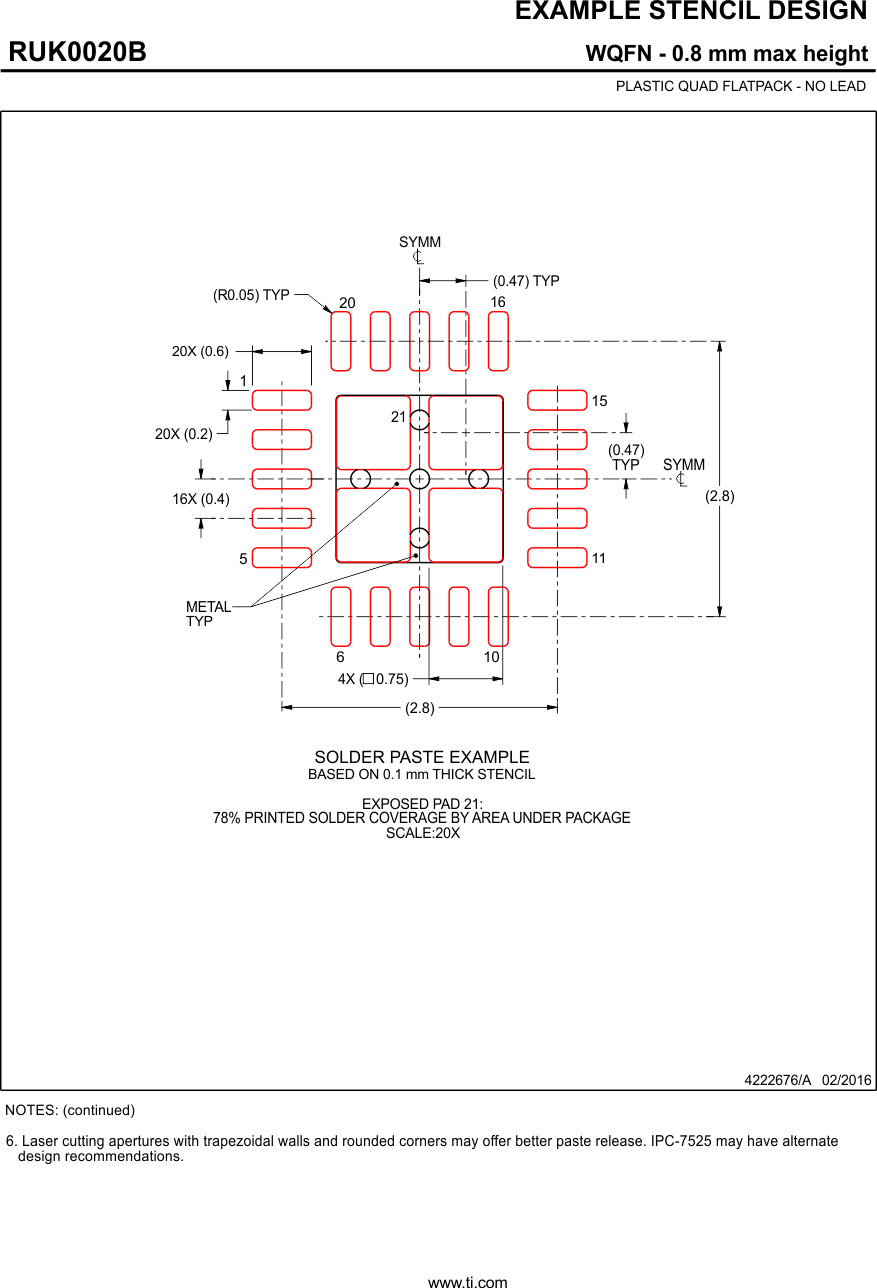
RUK|20
サーマルパッド・メカニカル・データ
発注情報
jajsp40a_pm
11.1
Mechanical Data