JAJSIN4D October   2003  – February 2020 ADS1204

PRODUCTION DATA.  

  1. 特長
  2. アプリケーション
  3. 概要
    1.     機能ブロック図
  4. 改訂履歴
  5. Pin Configuration and Functions
    1.     Pin Functions
  6. Specifications
    1. 6.1 Absolute Maximum Ratings
    2. 6.2 ESD Ratings
    3. 6.3 Recommended Operating Conditions
    4. 6.4 Thermal Information
    5. 6.5 Electrical Characteristics
    6. 6.6 Timing Requirements: 5.0 V
    7. 6.7 Timing Requirements: 3.0 V
    8. 6.8 Typical Characteristics
  7. Detailed Description
    1. 7.1 Overview
    2. 7.2 Functional Block Diagram
    3. 7.3 Feature Description
      1. 7.3.1 Analog Input Stage
        1. 7.3.1.1 Analog Input
        2. 7.3.1.2 Modulator
      2. 7.3.2 Digital Output
      3. 7.3.3 Equivalent Input Circuits
    4. 7.4 Device Functional Modes
  8. Application and Implementation
    1. 8.1 Application Information
      1. 8.1.1 Filter Usage
  9. Power Supply Recommendations
    1. 9.1 Power-Supply Sequencing
    2. 9.2 Power-Supply Decoupling
  10. 10Layout
    1. 10.1 Layout Guidelines
    2. 10.2 Layout Example
  11. 11デバイスおよびドキュメントのサポート
    1. 11.1 ドキュメントの更新通知を受け取る方法
    2. 11.2 サポート・リソース
    3. 11.3 商標
    4. 11.4 静電気放電に関する注意事項
    5. 11.5 Glossary
  12. 12メカニカル、パッケージ、および注文情報

パッケージ・オプション

メカニカル・データ(パッケージ|ピン)
サーマルパッド・メカニカル・データ
発注情報

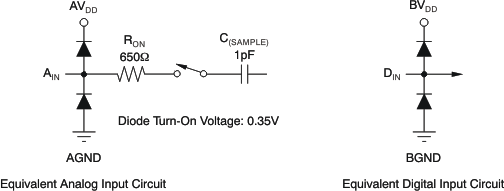
Equivalent Input Circuits

Figure 31 shows equivalent circuits for the analog input and digital outputs.
ADS1204 equiv_cir_bas301.gif

NOTE:

The thermal pad is internally connected to the substrate. This pad can be connected to the analog ground or left floating. Keep the thermal pad separate from the digital ground, if possible.
Figure 31. Equivalent Input Circuits