JAJSIN4D October 2003 – February 2020 ADS1204
PRODUCTION DATA.
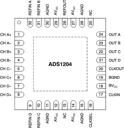
5 Pin Configuration and Functions
32-Pin VQFN
Top View

NOTE:
The thermal pad is internally connected to the substrate. This pad can be connected to the analog ground or left floating. Keep the thermal pad separate from the digital ground, if possible.Pin Functions
| PIN | I/O(1) | DESCRIPTION | |
|---|---|---|---|
| NAME | NO. | ||
| CH A+ | 1 | AI | Analog input of channel A: noninverting input |
| CH A– | 2 | AI | Analog input of channel A: inverting input |
| CH B+ | 3 | AI | Analog input of channel B: noninverting input |
| CH B– | 4 | AI | Analog input of channel B: inverting input |
| CH C– | 5 | AI | Analog input of channel C: inverting input |
| CH C+ | 6 | AI | Analog input of channel C: noninverting input |
| CH D– | 7 | AI | Analog input of channel D: inverting input |
| CH D+ | 8 | AI | Analog input of channel D: noninverting input |
| REFIN D | 9 | AI | Reference voltage input of channel D: pin for external reference voltage |
| REFIN C | 10 | AI | Reference voltage input of channel C: pin for external reference voltage |
| AGND | 11 | — | Analog ground |
| AVDD | 12 | P | Analog power supply; nominal 5 V |
| NC | 13 | — | No connection; this pin is left unconnected |
| AVDD | 14 | P | Analog power supply; nominal 5 V |
| AGND | 15 | — | Analog ground |
| CLKSEL | 16 | I | Clock select between internal clock (CLKSEL = 1) or external clock (CLKSEL = 0) |
| CLKIN | 17 | I | External clock input |
| BVDD | 18 | P | Digital interface power supply; from 2.7 V to 5.5 V |
| BGND | 19 | — | Interface ground |
| CLKOUT | 20 | O | System clock output |
| OUT D | 21 | O | Bit stream from channel D modulator |
| OUT C | 22 | O | Bit stream from channel C modulator |
| OUT B | 23 | O | Bit stream from channel B modulator |
| OUT A | 24 | O | Bit stream from channel A modulator |
| NC | 25 | — | No connection; this pin is left unconnected |
| AGND | 26 | — | Analog ground |
| AVDD | 27 | P | Analog power supply; nominal 5 V |
| REFOUT | 28 | AO | Reference voltage output: output pin of the internal reference source; nominal 2.5 V |
| AVDD | 29 | P | Analog power supply; nominal 5 V |
| AGND | 30 | — | Analog ground |
| REFIN B | 31 | AI | Reference voltage input of channel B: pin for external reference voltage |
| REFIN A | 32 | AI | Reference voltage input of channel A: pin for external reference voltage |
(1) AI = analog input; AO = analog output; I = input; O = output; P = power supply.