JAJSHL9A June   2019  – January 2021 ADS125H01

PRODUCTION DATA  

  1. 特長
  2. アプリケーション
  3. 概要
  4. Revision History
  5. Device Comparison Table
  6. Pin Configuration and Functions
  7. Specifications
    1. 7.1 Absolute Maximum Ratings
    2. 7.2 ESD Ratings
    3. 7.3 Recommended Operating Conditions
    4. 7.4 Thermal Information
    5. 7.5 Electrical Characteristics
    6. 7.6 Timing Requirements
    7. 7.7 Switching Characteristics
    8. 7.8 Timing Diagrams
    9. 7.9 Typical Characteristics
  8. Parameter Measurement Information
    1. 8.1 Noise Performance
  9. Detailed Description
    1. 9.1 Overview
    2. 9.2 Functional Block Diagram
    3. 9.3 Feature Description
      1. 9.3.1 Input Voltage Range
      2. 9.3.2 Analog Inputs (AINP, AINN)
        1. 9.3.2.1 ESD Diodes
        2. 9.3.2.2 Input Switch
      3. 9.3.3 Programmable Gain Amplifier (PGA)
        1. 9.3.3.1 PGA Operating Range
        2. 9.3.3.2 PGA Monitors
      4. 9.3.4 Reference Voltage
        1. 9.3.4.1 Reference Monitor
      5. 9.3.5 ADC Modulator
      6. 9.3.6 Digital Filter
        1. 9.3.6.1 Sinc Filter Mode
          1. 9.3.6.1.1 Sinc Filter Frequency Response
        2. 9.3.6.2 FIR Filter
        3. 9.3.6.3 50-Hz and 60-Hz Normal-Mode Rejection
    4. 9.4 Device Functional Modes
      1. 9.4.1 Conversion Control
        1. 9.4.1.1 Continuous-Conversion Mode
        2. 9.4.1.2 Pulse-Conversion Mode
        3. 9.4.1.3 Conversion Latency
        4. 9.4.1.4 Start-Conversion Delay
      2. 9.4.2 Clock Mode
      3. 9.4.3 Reset
        1. 9.4.3.1 Power-On Reset
        2. 9.4.3.2 Reset by RESETPin
        3. 9.4.3.3 Reset by Command
      4. 9.4.4 Calibration
        1. 9.4.4.1 Offset and Full-Scale Calibration
          1. 9.4.4.1.1 Offset Calibration Registers
          2. 9.4.4.1.2 Full-Scale Calibration Registers
        2. 9.4.4.2 Offset Calibration Command (OFSCAL)
        3. 9.4.4.3 Full-Scale Calibration Command (GANCAL)
        4. 9.4.4.4 Calibration Command Procedure
        5. 9.4.4.5 User Calibration Procedure
    5. 9.5 Programming
      1. 9.5.1 Serial Interface
        1. 9.5.1.1 Chip-Select Pins (CS1 and CS2)
        2. 9.5.1.2 Serial Clock (SCLK)
        3. 9.5.1.3 Data Input (DIN)
        4. 9.5.1.4 Data Output/Data Ready (DOUT/DRDY)
      2. 9.5.2 Data Ready (DRDY)
        1. 9.5.2.1 DRDY in Continuous-Conversion Mode
        2. 9.5.2.2 DRDY in Pulse-Conversion Mode
        3. 9.5.2.3 Data Ready by Software Polling
      3. 9.5.3 Conversion Data
        1. 9.5.3.1 Status Byte (STATUS0)
        2. 9.5.3.2 Conversion Data Format
      4. 9.5.4 Cyclic Redundancy Check (CRC)
      5. 9.5.5 Commands
        1. 9.5.5.1  General Command Format
        2. 9.5.5.2  NOP Command
        3. 9.5.5.3  RESET Command
        4. 9.5.5.4  START Command
        5. 9.5.5.5  STOP Command
        6. 9.5.5.6  RDATA Command
        7. 9.5.5.7  OFSCAL Command
        8. 9.5.5.8  GANCAL Command
        9. 9.5.5.9  RREG Command
        10. 9.5.5.10 WREG Command
    6. 9.6 Register Map
      1. 9.6.1  Device Identification (ID) Register (address = 00h) [reset = 4xh]
      2. 9.6.2  Main Status (STATUS0) Register (address = 01h) [reset = 01h]
      3. 9.6.3  Mode 0 (MODE0) Register (address = 02h) [reset = 24h]
      4. 9.6.4  Mode 1 (MODE1) Register (address = 03h) [reset = 01h]
      5. 9.6.5  Reserved (RESERVED) Register (address = 04h) [reset = 00h]
      6. 9.6.6  Mode 3 (MODE3) Register (address = 05h) [reset = 00h]
      7. 9.6.7  Reference Configuration (REF) Register (address = 06h) [reset = 05h]
      8. 9.6.8  Offset Calibration (OFCALx) Registers (address = 07h, 08h, 09h) [reset = 00h, 00h, 00h]
      9. 9.6.9  Full-Scale Calibration (FSCALx) Registers (address = 0Ah, 0Bh, 0Ch) [reset = 00h, 00h, 40h]
      10. 9.6.10 Reserved (RESERVED) Register (address = 0Dh) [reset = FFh]
      11. 9.6.11 Reserved (RESERVED) Register (address = 0Eh) [reset = 00h]
      12. 9.6.12 Reserved (RESERVED) Register (address = 0Fh) [reset = 00h]
      13. 9.6.13 MODE4 (MODE4) Register (address = 10h) [reset = 50h]
      14. 9.6.14 PGA Alarm (STATUS1) Register (address = 11h) [reset = xxh]
      15. 9.6.15 Status 2 (STATUS2) Register (address = 12h) [reset = 0xh]
  10. 10Application and Implementation
    1. 10.1 Application Information
      1. 10.1.1 Example to Determine the PGA Linear Operating Range
      2. 10.1.2 Input Signal Rate of Change (dV/dt)
      3. 10.1.3 Unused Inputs and Outputs
    2. 10.2 Typical Application
      1. 10.2.1 Design Requirements
      2. 10.2.2 Detailed Design Procedure
      3. 10.2.3 Application Curve
  11. 11Power Supply Recommendations
    1. 11.1 Power-Supply Decoupling
    2. 11.2 Analog Power-Supply Clamp
    3. 11.3 Power-Supply Sequencing
  12. 12Layout
    1. 12.1 Layout Guidelines
    2. 12.2 Layout Example
  13. 13Device and Documentation Support
    1. 13.1 Documentation Support
      1. 13.1.1 Related Documentation
    2. 13.2 ドキュメントの更新通知を受け取る方法
    3. 13.3 サポート・リソース
    4. 13.4 Trademarks
    5. 13.5 静電気放電に関する注意事項
    6. 13.6 用語集
  14. 14Mechanical, Packaging, and Orderable Information

パッケージ・オプション

メカニカル・データ(パッケージ|ピン)
サーマルパッド・メカニカル・データ
発注情報

Typical Application

Figure 10-1 illustrates an example of the ADS125H01 used in a ±10-V analog input programmable logic controller (PLC) module. The ADC inputs are protected by external ESD diodes to provide system-level protection. The external 100-MΩ resistor is used to pull the positive analog input to 15 V if the field-wiring connection is open or the transmitter connected the ADC inputs has a failed open circuit. A failed input results in a full-scale code value.

The signal from the transmitter is filtered to remove EMI and RFI interference to enhance noise immunity. The resistor also serves to limit input current in the event of a DC overvoltage, including if the module loses power while the input signal is present. The negative input is connected to AINN, which is also connected to AGND. Connection to AGND is necessary if the sensor power supply is not referenced to the ADC ground.

The input configuration is single-ended with the input voltage driven to 0 V and –10 V relative to AINN (AGND).

The reference voltage is applied to the REFP and REFN pins. A 100-kΩ resistor biases the differential reference voltage to 0 V when either reference input is open circuit. With the resistor, a failed or missing reference voltage is detected by the internal monitor.

The internal oscillator is selected by grounding the CLKIN pin. The serial interface and digital control lines of the ADC connect to the host.

The Zener diode clamps the high-voltage supply (HV_AVDD – HV_AVSS) to 40 V to provide overvoltage protection if an input signal is applied with module power off.
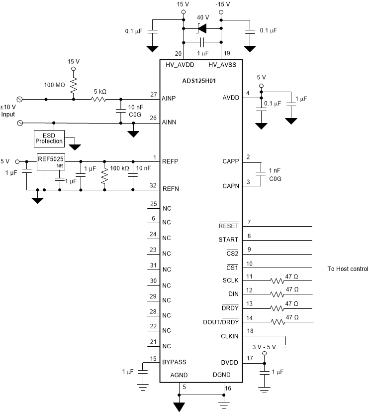
GUID-BC22786D-B54A-4C63-8761-3B27BAB25C6E-low.gif Figure 10-1 ±10-V Analog Input PLC Module