JAJSHL9A June 2019 – January 2021 ADS125H01
PRODUCTION DATA
- 1 特長
- 2 アプリケーション
- 3 概要
- 4 Revision History
- 5 Device Comparison Table
- 6 Pin Configuration and Functions
- 7 Specifications
- 8 Parameter Measurement Information
-
9 Detailed Description
- 9.1 Overview
- 9.2 Functional Block Diagram
- 9.3 Feature Description
- 9.4 Device Functional Modes
- 9.5 Programming
- 9.6
Register Map
- 9.6.1 Device Identification (ID) Register (address = 00h) [reset = 4xh]
- 9.6.2 Main Status (STATUS0) Register (address = 01h) [reset = 01h]
- 9.6.3 Mode 0 (MODE0) Register (address = 02h) [reset = 24h]
- 9.6.4 Mode 1 (MODE1) Register (address = 03h) [reset = 01h]
- 9.6.5 Reserved (RESERVED) Register (address = 04h) [reset = 00h]
- 9.6.6 Mode 3 (MODE3) Register (address = 05h) [reset = 00h]
- 9.6.7 Reference Configuration (REF) Register (address = 06h) [reset = 05h]
- 9.6.8 Offset Calibration (OFCALx) Registers (address = 07h, 08h, 09h) [reset = 00h, 00h, 00h]
- 9.6.9 Full-Scale Calibration (FSCALx) Registers (address = 0Ah, 0Bh, 0Ch) [reset = 00h, 00h, 40h]
- 9.6.10 Reserved (RESERVED) Register (address = 0Dh) [reset = FFh]
- 9.6.11 Reserved (RESERVED) Register (address = 0Eh) [reset = 00h]
- 9.6.12 Reserved (RESERVED) Register (address = 0Fh) [reset = 00h]
- 9.6.13 MODE4 (MODE4) Register (address = 10h) [reset = 50h]
- 9.6.14 PGA Alarm (STATUS1) Register (address = 11h) [reset = xxh]
- 9.6.15 Status 2 (STATUS2) Register (address = 12h) [reset = 0xh]
- 10Application and Implementation
- 11Power Supply Recommendations
- 12Layout
- 13Device and Documentation Support
- 14Mechanical, Packaging, and Orderable Information
パッケージ・オプション
メカニカル・データ(パッケージ|ピン)
- RHB|32
サーマルパッド・メカニカル・データ
- RHB|32
発注情報
8.1 Noise Performance
Noise performance depends on the device configuration: data rate, input gain, and digital filter mode. Two significant factors affecting noise performance are data rate and input gain. Decreasing the data rate lowers the noise because the measurement bandwidth is reduced. Increasing the gain reduces noise (when noise is treated as an input-referred quantity) because the noise of the PGA is lower than that of the ADC. Noise performance also depends on the digital filter mode. As the digital filter order is increased, the bandwidth decreases, which results in lower noise.
Figure 8-1 shows noise data versus data rate as input-referred values (µVRMS) in gains 0.125 to 2, (corresponding input ranges of ±20 V to ±1.25 V) in the sinc3 filter mode. Figure 8-2 shows noise data versus data rate as input-referred values (µVRMS) in gains 4 to 128, (corresponding input ranges of ±625 mV to ±19.5 mV) in the sinc3 filter mode. The noise data represent typical ADC performance at TA = 25°C and the 2.5-V reference voltage.
Peak-to-peak noise performance is typically 6.6 times the RMS value. Relative to the noise in the sinc3 filter mode, noise typically increases 30% in the finite-impulse response (FIR) and sinc1 filter mode because of the increased bandwidth of the sinc1 and FIR modes. Noise typically decreases 6% in the sinc4 filter mode because of the decreased bandwidth of the sinc4 filter mode.
The noise data are the standard deviation of the ADC data scaled in microvolts. The data are acquired with inputs shorted and based on consecutive ADC readings for a period of ten seconds or 8192 data points, whichever occurs first. Because of the statistical nature of noise, repeated measurements may yield higher or lower noise results.
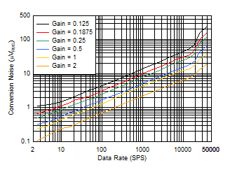
| Gain = 0.125 to 2,
VREF = 2.5 V, sinc3 filter (sinc5 filter for fDATA ≥ 14.4 kSPS) |
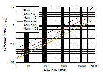
| Gain = 4 to 128,
VREF = 2.5 V, sinc3 filter (sinc5 filter for fDATA ≥ 14.4 kSPS) |
ADC noise performance can also be expressed as effective resolution and noise-free resolution (bits). Effective resolution is based on the RMS value of the noise data and noise-free resolution is based on the peak-to-peak noise data; therefore, the noise-free resolution is the resolution with no code flicker. Equation 1 is used to compute effective resolution based on the noise values plots of Figure 8-1 and Figure 8-2.
where:
- FSR = Full-scale range = 2 VREF / Gain
- en = Input-referred noise (RMS value for effective resolution, peak-to-peak value for noise-free resolution)
For example, using full-scale range = ±13.3 V, data rate = 20 SPS, and sinc3 filter mode, the RMS noise value (from Figure 8-1) is 2.1 µV. The effective resolution is: 3.32 log (26.6 V / 2.1 µV) = 23.6 bits.
Figure 8-3 and Figure 8-4 show effective resolution (bits) versus data rate. Figure 8-5 and Figure 8-6 show noise-free resolution (bits) versus data rate. When fDATA ≤ 14.4 kSPS, effective resolution and noise-free resolution improve by 0.7 bits by increasing the reference voltage from 2.5 V to 4.096 V because of the increased input signal range.
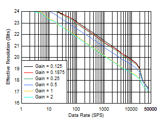
| Gain = 0.125 to 2,
VREF = 2.5 V, sinc3 filter (sinc5 filter for fDATA ≥ 14.4 kSPS) |
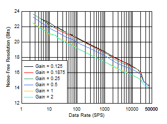
| Gain = 0.125 to 2,
VREF = 2.5 V, sinc3 filter (sinc5 filter for fDATA ≥ 14.4 kSPS) |
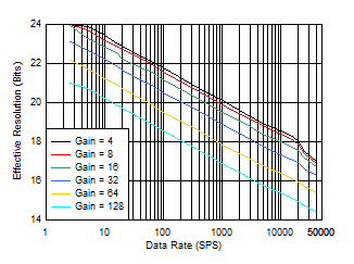
| Gain = 4 to 128,
VREF = 2.5 V, sinc3 filter mode (sinc5 filter for fDATA ≥ 14.4 kSPS) |
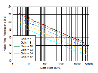
| Gain = 4 to 128,
VREF = 2.5 V, sinc3 filter (sinc5 filter for fDATA ≥ 14.4 kSPS) |