JAJSHL9A June 2019 – January 2021 ADS125H01
PRODUCTION DATA
- 1 特長
- 2 アプリケーション
- 3 概要
- 4 Revision History
- 5 Device Comparison Table
- 6 Pin Configuration and Functions
- 7 Specifications
- 8 Parameter Measurement Information
-
9 Detailed Description
- 9.1 Overview
- 9.2 Functional Block Diagram
- 9.3 Feature Description
- 9.4 Device Functional Modes
- 9.5 Programming
- 9.6
Register Map
- 9.6.1 Device Identification (ID) Register (address = 00h) [reset = 4xh]
- 9.6.2 Main Status (STATUS0) Register (address = 01h) [reset = 01h]
- 9.6.3 Mode 0 (MODE0) Register (address = 02h) [reset = 24h]
- 9.6.4 Mode 1 (MODE1) Register (address = 03h) [reset = 01h]
- 9.6.5 Reserved (RESERVED) Register (address = 04h) [reset = 00h]
- 9.6.6 Mode 3 (MODE3) Register (address = 05h) [reset = 00h]
- 9.6.7 Reference Configuration (REF) Register (address = 06h) [reset = 05h]
- 9.6.8 Offset Calibration (OFCALx) Registers (address = 07h, 08h, 09h) [reset = 00h, 00h, 00h]
- 9.6.9 Full-Scale Calibration (FSCALx) Registers (address = 0Ah, 0Bh, 0Ch) [reset = 00h, 00h, 40h]
- 9.6.10 Reserved (RESERVED) Register (address = 0Dh) [reset = FFh]
- 9.6.11 Reserved (RESERVED) Register (address = 0Eh) [reset = 00h]
- 9.6.12 Reserved (RESERVED) Register (address = 0Fh) [reset = 00h]
- 9.6.13 MODE4 (MODE4) Register (address = 10h) [reset = 50h]
- 9.6.14 PGA Alarm (STATUS1) Register (address = 11h) [reset = xxh]
- 9.6.15 Status 2 (STATUS2) Register (address = 12h) [reset = 0xh]
- 10Application and Implementation
- 11Power Supply Recommendations
- 12Layout
- 13Device and Documentation Support
- 14Mechanical, Packaging, and Orderable Information
パッケージ・オプション
メカニカル・データ(パッケージ|ピン)
- RHB|32
サーマルパッド・メカニカル・データ
- RHB|32
発注情報
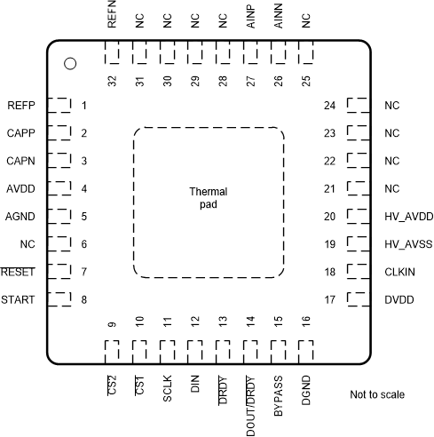
6 Pin Configuration and Functions
 Figure 6-1
RHB Package,
32-Pin VQFN,
Top View
Table 6-1 Pin Functions
| NO. | NAME | I/O | DESCRIPTION |
|---|---|---|---|
| 1 | REFP | Analog input | Positive reference input |
| 2 | CAPP | Analog output | PGA output P; connect a 1-nF C0G dielectric capacitor from CAPP to CAPN |
| 3 | CAPN | Analog output | PGA output N; connect a 1-nF C0G dielectric capacitor from CAPP to CAPN |
| 4 | AVDD | Analog | Low-voltage analog power supply |
| 5 | AGND | Analog | Analog ground; connect to the ADC ground plane |
| 6 | NC | — | No connection; electrically float or tie to AGND |
| 7 | RESET | Digital input | Reset; active low |
| 8 | START | Digital input | Conversion start, active high |
| 9 | CS2 | Digital input | Serial interface chip-select 2 to select the PGA for communication |
| 10 | CS1 | Digital input | Serial interface chip-select 1 to select the ADC for communication |
| 11 | SCLK | Digital input | Serial interface shift clock |
| 12 | DIN | Digital input | Serial interface data input |
| 13 | DRDY | Digital output | Data ready; active low |
| 14 | DOUT/DRDY | Digital output | Serial interface data output or data-ready output, active low |
| 15 | BYPASS | Analog output | 2-V subregulator output; connect a 1-µF capacitor to DGND |
| 16 | DGND | Digital | Digital ground; connect to the ADC ground plane |
| 17 | DVDD | Digital | Digital power supply |
| 18 | CLKIN | Digital input | External clock input; connect to DGND for internal oscillator operation |
| 19 | HV_AVSS | Analog | High-voltage negative analog power supply |
| 20 | HV_AVDD | Analog | High-voltage positive analog power supply |
| 21 – 25 | NC | — | No connection; electrically float or tie to AGND |
| 26 | AINN | Analog input | Negative analog input |
| 27 | AINP | Analog input | Positive analog input |
| 28 – 31 | NC | — | No connection; electrically float or tie to AGND |
| 32 | REFN | Analog input | Negative reference input |
| Thermal pad | — | Exposed thermal pad; connect to DGND; see the recommended PCB land pattern at the end of the document | |