JAJSGG2C October 2018 – June 2019 ADS125H02
PRODUCTION DATA.
- 1 特長
- 2 アプリケーション
- 3 概要
- 4 改訂履歴
- 5 概要(続き)
- 6 Device Comparison Table
- 7 Pin Configuration and Functions
- 8 Specifications
- 9 Parameter Measurement Information
-
10Detailed Description
- 10.1 Overview
- 10.2 Functional Block Diagram
- 10.3 Feature Description
- 10.4 Device Functional Modes
- 10.5 Programming
- 10.6
Register Map
- 10.6.1 Device Identification (ID) Register (address = 00h) [reset = 6xh]
- 10.6.2 Main Status (STATUS0) Register (address = 01h) [reset = 01h]
- 10.6.3 Mode 0 (MODE0) Register (address = 02h) [reset = 24h]
- 10.6.4 Mode 1 (MODE1) Register (address = 03h) [reset = 01h]
- 10.6.5 Mode 2 (MODE2) Register (address = 04h) [reset = 00h]
- 10.6.6 Mode 3 (MODE3) Register (address = 05h) [reset = 00h]
- 10.6.7 Reference Configuration (REF) Register (address = 06h) [reset = 05h]
- 10.6.8 Offset Calibration (OFCALx) Registers (address = 07h, 08h, 09h) [reset = 00h, 00h, 00h]
- 10.6.9 Full-Scale Calibration (FSCALx) Registers (address = 0Ah, 0Bh, 0Ch) [reset = 00h, 00h, 40h]
- 10.6.10 Current Source Multiplexer (I_MUX) Register (address = 0Dh) [reset = FFh]
- 10.6.11 Current Source Magnitude (I_MAG) Register (address = 0Eh) [reset = 00h]
- 10.6.12 Reserved (RESERVED) Register (address = 0Fh) [reset = 00h]
- 10.6.13 MODE4 (MODE4) Register (address = 10h) [reset = 50h]
- 10.6.14 PGA Alarm (STATUS1) Register (address = 11h) [reset = xxh]
- 10.6.15 Status 2 (STATUS2) Register (address = 12h) [reset = 0xh]
- 11Application and Implementation
- 12Power Supply Recommendations
- 13Layout
- 14デバイスおよびドキュメントのサポート
- 15メカニカル、パッケージ、および注文情報
パッケージ・オプション
メカニカル・データ(パッケージ|ピン)
- RHB|32
サーマルパッド・メカニカル・データ
- RHB|32
発注情報
8.7 Switching Characteristics
over operating the ambient temperature range and DVDD = 2.7 V to 5.25 V, and DOUT/DRDY load = 20 pF || 100 kΩ to DGND (unless otherwise noted)| PARAMETER | TEST CONDITIONS | MIN | TYP | MAX | UNIT | |
|---|---|---|---|---|---|---|
| SERIAL INTERFACE | ||||||
| tw(DRH) | Pulse duration, DRDY high | 16 | 1 / fCLK | |||
| tp(CSDO) | Propagation delay time, CS1 or CS2 falling edge to DOUT/DRDY driven | 0 | 50 | ns | ||
| tp(SCDO1) | Propagation delay time, SCLK rising edge to valid DOUT/DRDY | 40 | ns | |||
| th(SCDO1) | Hold time, SCLK rising edge to invalid DOUT/DRDY | 0 | ns | |||
| th(SCDO2) | Hold time, last SCLK falling edge to invalid DOUT/DRDY data output function | 15 | ns | |||
| tp(SCDO2) | Propagation delay time, last SCLK falling edge to DOUT/DRDY data-ready function | 110 | ns | |||
| tp(CSDOZ) | Propagation delay time, CS1 or CS2 rising edge to DOUT/DRDY high impedance | 50 | ns | |||
| RESET | ||||||
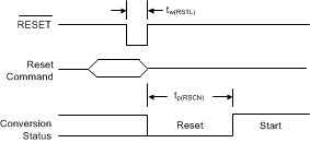
| tp(RSCN) | Propagation delay time, RESET rising edge or RESET command to conversion start | 512 | 1 / fCLK | |||
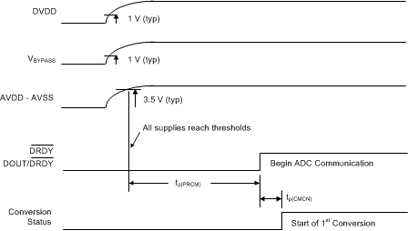
| tp(PRCM) | Propagation delay time, power-on threshold voltage to ADC communication | 216 | 1 / fCLK | |||
| tp(CMCN) | Propagation delay time, ADC communication to conversion start | 512 | 1 / fCLK | |||
| CONVERSION CONTROL | ||||||
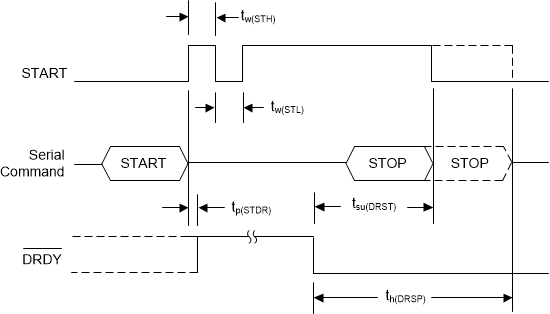
| tp(STDR) | Propagation delay time, START pin high or START command to DRDY high | 2 | 1 / fCLK | |||
 Figure 1. Serial Interface Timing Requirements
1. DRDY is the data-ready function in the interval between CS1 low and the first SCLK rising edge, and in the interval between the last SCLK falling edge of the command to CS1 high. DOUT is the data output function during the data read operation.
Figure 2. Serial Interface Switching Characteristics  Figure 3. Conversion Control Timing Requirements
  Figure 4. Power-Up Characteristics
  Figure 5. RESET Pin and Reset Command Timing Requirements