SBAS459K January 2010 – August 2015 ADS1294 , ADS1294R , ADS1296 , ADS1296R , ADS1298 , ADS1298R
PRODUCTION DATA.
- 1 Features
- 2 Applications
- 3 Description
- 4 Revision History
- 5 Device Comparison
- 6 Pin Configuration and Functions
- 7 Specifications
- 8 Parameter Measurement Information
-
9 Detailed Description
- 9.1 Overview
- 9.2 Functional Block Diagram
- 9.3
Feature Description
- 9.3.1
Analog Functionality
- 9.3.1.1 EMI Filter
- 9.3.1.2 Analog Input Structure
- 9.3.1.3
Input Multiplexer
- 9.3.1.3.1 Device Noise Measurements
- 9.3.1.3.2 Test Signals (TestP and TestN)
- 9.3.1.3.3 Auxiliary Differential Input (TESTP_PACE_OUT1, TESTN_PACE_OUT2)
- 9.3.1.3.4 Temperature Sensor (TempP, TempN)
- 9.3.1.3.5 Supply Measurements (MVDDP, MVDDN)
- 9.3.1.3.6 Lead-Off Excitation Signals (LoffP, LoffN)
- 9.3.1.3.7 Auxiliary Single-Ended Input
- 9.3.1.4 Analog Input
- 9.3.1.5 PGA Settings and Input Range
- 9.3.1.6 Reference
- 9.3.1.7
ECG-Specific Functions
- 9.3.1.7.1 Input Multiplexer (Rerouting The Right Leg Drive Signal)
- 9.3.1.7.2 Input Multiplexer (Measuring The Right Leg Drive Signal)
- 9.3.1.7.3 Wilson Central Terminal (WCT) and Chest Leads
- 9.3.1.7.4 Lead-Off Detection
- 9.3.1.7.5 RLD Lead-Off
- 9.3.1.7.6 Right Leg Drive (RLD) DC Bias Circuit
- 9.3.1.7.7 Pace Detect
- 9.3.1.7.8 Respiration
- 9.3.2 Digital Functionality
- 9.3.1
Analog Functionality
- 9.4 Device Functional Modes
- 9.5
Programming
- 9.5.1 SPI Interface
- 9.5.2
SPI Command Definitions
- 9.5.2.1 WAKEUP: Exit Standby Mode
- 9.5.2.2 STANDBY: Enter Standby Mode
- 9.5.2.3 RESET: Reset Registers to Default Values
- 9.5.2.4 START: Start Conversions
- 9.5.2.5 STOP: Stop Conversions
- 9.5.2.6 RDATAC: Read Data Continuous
- 9.5.2.7 SDATAC: Stop Read Data Continuous
- 9.5.2.8 RDATA: Read Data
- 9.5.2.9 Sending Multibyte Commands
- 9.5.2.10 RREG: Read From Register
- 9.5.2.11 WREG: Write to Register
- 9.6
Register Maps
- 9.6.1
Register Descriptions
- 9.6.1.1 ID: ID Control Register (address = 00h) (reset = xxh)
- 9.6.1.2 CONFIG1: Configuration Register 1 (address = 01h) (reset = 06h)
- 9.6.1.3 CONFIG2: Configuration Register 2 (address = 02h) (reset = 40h)
- 9.6.1.4 CONFIG3: Configuration Register 3 (address = 03h) (reset = 40h)
- 9.6.1.5 LOFF: Lead-Off Control Register (address = 04h) (reset = 00h)
- 9.6.1.6 CHnSET: Individual Channel Settings (n = 1 to 8) (address = 05h to 0Ch) (reset = 00h)
- 9.6.1.7 RLD_SENSP: RLD Positive Signal Derivation Register (address = 0Dh) (reset = 00h)
- 9.6.1.8 RLD_SENSN: RLD Negative Signal Derivation Register (address = 0Eh) (reset = 00h)
- 9.6.1.9 LOFF_SENSP: Positive Signal Lead-Off Detection Register (address = 0Fh) (reset = 00h)
- 9.6.1.10 LOFF_SENSN: Negative Signal Lead-Off Detection Register (address = 10h) (reset = 00h)
- 9.6.1.11 LOFF_FLIP: Lead-Off Flip Register (address = 11h) (reset = 00h)
- 9.6.1.12 LOFF_STATP: Lead-Off Positive Signal Status Register (address = 12h) (reset = 00h)
- 9.6.1.13 LOFF_STATN: Lead-Off Negative Signal Status Register (address = 13h) (reset = 00h)
- 9.6.1.14 GPIO: General-Purpose I/O Register (address = 14h) (reset = 0Fh)
- 9.6.1.15 PACE: Pace Detect Register (address = 15h) (reset = 00h)
- 9.6.1.16 RESP: Respiration Control Register (address = 16h) (reset = 00h)
- 9.6.1.17 CONFIG4: Configuration Register 4 (address = 17h) (reset = 00h)
- 9.6.1.18 WCT1: Wilson Central Terminal and Augmented Lead Control Register (address = 18h) (reset = 00h)
- 9.6.1.19 WCT2: Wilson Central Terminal Control Register (address = 18h) (reset = 00h)
- 9.6.1
Register Descriptions
- 10Application and Implementation
- 11Power Supply Recommendations
- 12Layout
- 13Device and Documentation Support
- 14Mechanical, Packaging, and Orderable Information
パッケージ・オプション
メカニカル・データ(パッケージ|ピン)
サーマルパッド・メカニカル・データ
- PAG|64
発注情報
9 Detailed Description
9.1 Overview
NOTE
The ADS129xR channel performance differs from the ADS129x in regards to respiration circuitry found on channel one. Unless otherwise noted, ADS129x refers to all specifications and functional descriptions of the ADS1294, ADS1296, ADS1298, ADS1294R, ADS1296R, and ADS1298R. ADS129xR refers to all specifications and functional descriptions of only the ADS1294R, ADS1296R, and ADS1298R.
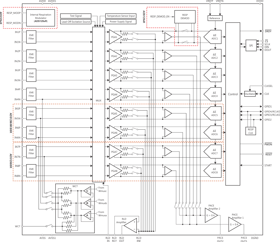
The ADS129x are low-power, multichannel, simultaneously-sampling, 24-bit delta-sigma (ΔΣ) analog-to-digital converters (ADCs) with integrated programmable gain amplifiers (PGAs). These devices incorporate various ECG-specific functions that make them well-suited for scalable electrocardiogram (ECG), electroencephalography (EEG), and electromyography (EMG) applications. These devices are also used in high-performance, multichannel data acquisition systems by powering down the ECG-specific circuitry.
The ADS129x have a highly-programmable multiplexer (mux) that allows for temperature, supply, input short, and RLD measurements. Additionally, the mux allows any of the input electrodes to be programmed as the patient reference drive. The PGA gain is chosen from one of seven settings: 1, 2, 3, 4, 6, 8, or 12. The ADCs in the device offer data rates from 250 SPS to 32 kSPS. Communicate with the device by using an SPI-compatible interface. The device provides four GPIO pins for general use. Synchronize multiple devices by using the START pin.
Program the internal reference to either 2.4 V or 4 V. The internal oscillator generates a 2.048-MHz clock. The versatile right-leg drive (RLD) block allows for choosing the average of any combination of electrodes to generate the patient drive signal. Lead-off detection is accomplished either by using a pullup or pulldown resistor, or a current source or sink. An internal ac lead-off detection feature is also available. These devices support both hardware pace detection and software pace detection. Use the Wilson central terminal (WCT) block to generate the WCT point of the standard 12-lead ECG.
Additionally, the ADS129xR provide options for an internal respiration modulator and a demodulator circuit in the signal path of channel 1.
9.3 Feature Description
This section discusses the details of the ADS129x internal functional elements. The analog blocks are reviewed first, followed by the digital interface. Blocks implementing ECG-specific functions are covered at the end.
Throughout this document, fCLK denotes the frequency of the signal at the CLK pin, tCLK denotes the period of the signal at the CLK pin, fDR denotes the output data rate, tDR denotes the time period of the output data, and fMOD denotes the modulator input sampling frequency.
9.3.1 Analog Functionality
9.3.1.1 EMI Filter
An RC filter at the input acts as an EMI filter on all channels. The –3-dB filter bandwidth is approximately 3 MHz.
9.3.1.2 Analog Input Structure
The analog input of the ADS129x is shown in Figure 24.
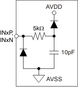 Figure 24. Analog Input Protection Circuit
9.3.1.3 Input Multiplexer
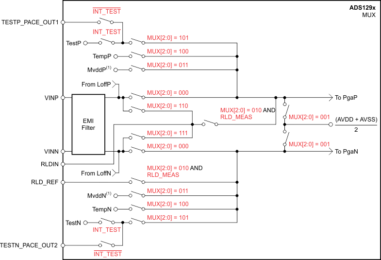
The ADS129x input multiplexers are very flexible and provide many configurable signal-switching options. Figure 25 shows the multiplexer on a single channel of the device. The device has eight blocks, one for each channel. TEST_PACE_OUT1, TEST_PACE_OUT2, and RLD_IN are common to all eight blocks. VINP and VINN are separate for each of the eight blocks. This flexibility allows for significant device and subsystem diagnostics, calibration, and configuration. Select the switch settings for each channel by writing 1 to the appropriate values to the CHnSET[2:0] register (see the CHnSET register for details) and the RLD_MEAS bit in the CONFIG3 register (see the CONFIG3 register for details). More details of the ECG-specific features of the multiplexer are presented in the Input Multiplexer (Rerouting The Right Leg Drive Signal) subsection of the ECG-Specific Functions section.
9.3.1.3.1 Device Noise Measurements
Setting CHnSET[2:0] = 001 sets the common-mode voltage of (AVDD – AVSS) / 2 to both inputs of the channel. Use this setting to test the inherent noise of the device.
9.3.1.3.2 Test Signals (TestP and TestN)
Setting CHnSET[2:0] = 101 provides internally-generated test signals for use in subsystem verification at power up. This functionality allows the entire signal chain to be tested. Although the test signals are similar to the CAL signals described in the IEC60601-2-51 specification, this feature is not intended for use in compliance testing.
Use register settings to control the test signals (see the CONFIG2: Configuration Register 2 (address = 02h) (reset = 40h) section for details). The TEST_AMP bit controls the signal amplitude, and the TEST_FREQ bits control switching at the required frequency.
The test signals are multiplexed and transmitted out of the device at the TESTP_PACE_OUT1 and TESTN_PACE_OUT2 pins. A bit register (CONFIG2.INT_TEST = 0) deactivates the internal test signals so that the test signal can be driven externally. This feature allows the calibration of multiple devices with the same signal. The test signal feature cannot be used in conjunction with the external hardware pace feature (see the External Hardware Approach section for details).
9.3.1.3.3 Auxiliary Differential Input (TESTP_PACE_OUT1, TESTN_PACE_OUT2)
When hardware pace detection is not used, the TESTP_PACE_OUT1 and TESPN_PACE_OUT2 signals can be used as a multiplexed differential input channel. These inputs can be multiplexed to any of the eight channels. The performance of the differential input signal fed through these pins is identical to the normal channel performance.
9.3.1.3.4 Temperature Sensor (TempP, TempN)
The ADS129x contain an on-chip temperature sensor. This sensor uses two internal diodes with one diode having a current density 16x that of the other, as shown in Figure 26. The difference in current densities of the diodes yields a difference in voltage that is proportional to absolute temperature.
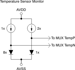 Figure 26. Measurement of the Temperature Sensor in the Input
As a result of the low thermal resistance of the package to the printed circuit board (PCB), the internal sensor tracks the PCB temperature closely. Self-heating of the ADS129x causes a higher reading than the temperature of the surrounding PCB.
The scale factor of Equation 1 converts the temperature reading to °C. Before using this equation, scale the the temperature reading code to μV.

9.3.1.3.5 Supply Measurements (MVDDP, MVDDN)
Setting CHnSET[2:0] = 011 sets the channel inputs to different supply voltages of the device.
For channels 1, 2, 5, 6, 7, and 8, (MVDDP – MVDDN) = [0.5 × (AVDD – AVSS)]
For channels 3 and 4, (MVDDP – MVDDN) = DVDD / 4.
To avoid saturating the PGA while measuring power supplies, set the gain to 1.
For example, if AVDD = 2.5 V and AVSS = –2.5 V, then the measurement result is 2.5 V.
9.3.1.3.6 Lead-Off Excitation Signals (LoffP, LoffN)
The lead-off excitation signals are fed into the multiplexer before the switches. The comparators that detect the lead-off condition are also connected to the multiplexer block before the switches. For a detailed description of the lead-off block, refer to the Lead-Off Detection section.
9.3.1.3.7 Auxiliary Single-Ended Input
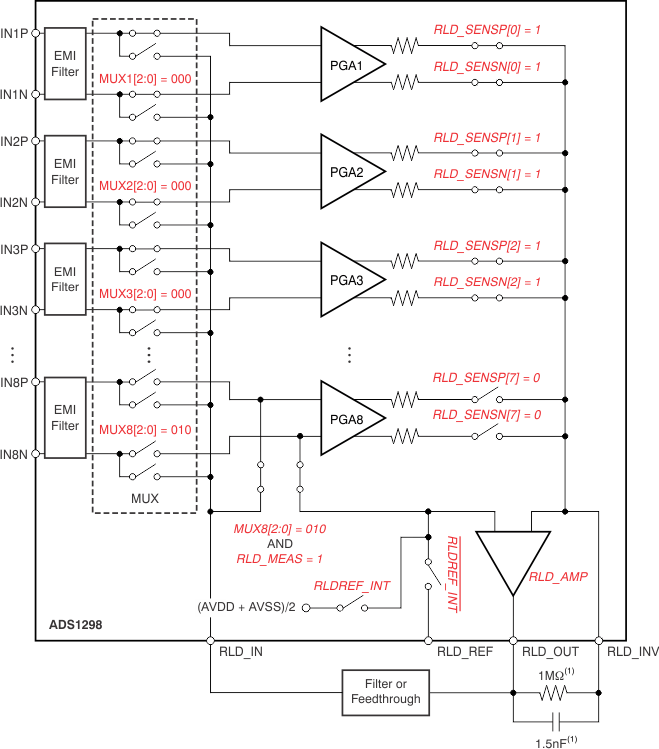
The RLD_IN pin is primarily used for routing the right leg drive (RLD) signal to any of the electrodes in case the RLD electrode falls off. However, the RLD_IN pin can be used as a multiple single-ended input channel. The signal at the RLD_IN pin can be measured with respect to the voltage at the RLD_REF pin using any of the eight channels. This measurement is done by setting the channel multiplexer setting to 010, and the RLD_MEAS bit of the CONFIG3 register to 1.
9.3.1.4 Analog Input
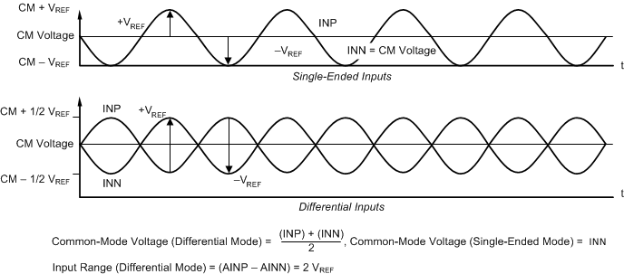
The analog input to the ADS129x is fully differential. Assuming PGA = 1, the differential input (INP – INN) can span between –VREF to VREF. The absolute range for INP and INN must be between AVSS – 0.3 V and AVDD + 0.3 V. See Table 13 for an explanation of the correlation between the analog input and the digital codes. As shown in Figure 27 and Figure 28, there are two general methods of driving the analog input of the ADS129x: single-ended or differential. INP and INN are 180° out-of-phase in the differential input method. When the input is single-ended, the INN input is held at the common-mode voltage (CM), preferably at midsupply. The INP input swings around the same common-mode voltage and the peak-to-peak amplitude swings from CM – VREF to CM + VREF. When the input is differential, the common-mode is given by (INP + INN) / 2. Both the INP and INN inputs swing from CM + ½ VREF to CM – ½ VREF. For optimal performance, use the ADS129x devices in a differential configuration.
9.3.1.5 PGA Settings and Input Range
The PGA is a differential input and differential output amplifier, as shown in Figure 29. The PGA has seven gain settings (1, 2, 3, 4, 6, 8, and 12) that are set by writing to the CHnSET register (see the CHnSET: Individual Channel Settings (n = 1 to 8) (address = 05h to 0Ch) (reset = 00h) section). The ADS129x have CMOS inputs, and therefore have negligible current noise. Table 5 shows the typical values of bandwidths for various gain settings. Table 5 shows the small-signal bandwidth.
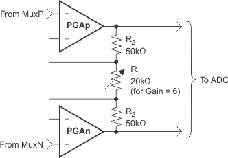 Figure 29. PGA Implementation
Table 5. PGA Gain versus Small-Signal Bandwidth
| GAIN | NOMINAL BANDWIDTH AT ROOM TEMPERATURE (kHz) |
|---|---|
| 1 | 237 |
| 2 | 146 |
| 3 | 127 |
| 4 | 96 |
| 6 | 64 |
| 8 | 48 |
| 12 | 32 |
The resistor string of the PGA that implements the gain has 120 kΩ of resistance for a gain of 6. This resistance provides a current path across the outputs of the PGA in the presence of a differential input signal. This current is in addition to the quiescent current specified for the device in the presence of a differential signal at the input.
9.3.1.5.1 Input Common-Mode Range
The usable input common-mode range of the front end depends on various parameters, including the maximum differential input signal, supply voltage, PGA gain, and more. This range is described in Equation 2:

where
- VMAX_DIFF = maximum differential signal at the input of the PGA
- CM = common-mode range
For example, If VDD = 3 V, gain = 6, and VMAX_DIFF = 350 mV, then 1.25 V < CM < 1.75 V.
9.3.1.5.2 Input Differential Dynamic Range
The differential (INP – INN) signal range depends on the analog supply and reference used in the system. This range is shown in Equation 3.
The 3-V supply, with a reference of 2.4 V and a gain of 6 for ECGs, is optimized for power with a differential input signal of approximately 300 mV. For higher dynamic range, use a 5-V supply with a reference of 4 V (set by the VREF_4V bit of the CONFIG3 register) to increase the differential dynamic range.
9.3.1.5.3 ADC Delta-Sigma Modulator
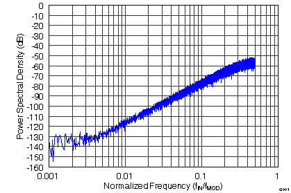
Each channel of the ADS129x has a 24-bit, delta-sigma ADC. This converter uses a second-order modulator optimized for low-power applications. The modulator samples the input signal at the rate of fMOD = fCLK / 4 for high-resolution (HR) mode and fMOD = fCLK / 8 for low-power (LP) mode. As in the case of any delta-sigma modulator, the noise of the ADS129x is shaped until fMOD / 2, as shown in Figure 30. Use the on-chip digital decimation filters, explained in the Digital Decimation Filter section, to filter out the noise at higher frequencies. These on-chip decimation filters also provide antialias filtering. This feature of the delta-sigma converters drastically reduces the complexity of the analog antialiasing filters that are typically needed with Nyquist ADCs.
9.3.1.6 Reference
Figure 31 shows a simplified block diagram of the ADS129x internal reference. The reference voltage is generated with respect to AVSS. When using the internal voltage reference, connect VREFN to AVSS.
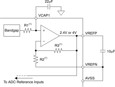
The external band-limiting capacitors determine the amount of reference noise contribution. For high-end ECG systems, choose capacitor values with a bandwidth that is limited to less than 10Hz, so that the reference noise does not dominate the system noise. When using a 3-V analog supply, set the internal reference to 2.4 V. For a 5-V analog supply, set the internal reference to 4 V by setting the VREF_4V bit in the CONFIG2 register.
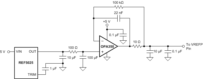
Alternatively, the internal reference buffer can be powered down and VREFP can be applied externally. Figure 32 shows a typical external reference drive circuitry. Power down is controlled by the PD_REFBUF bit in the CONFIG3 register. By default, the device wakes up in external reference mode.
9.3.1.7 ECG-Specific Functions
9.3.1.7.1 Input Multiplexer (Rerouting The Right Leg Drive Signal)
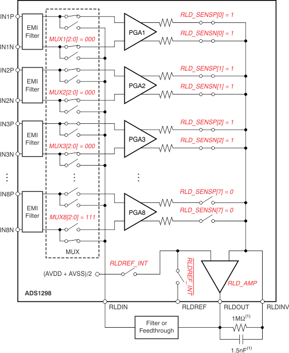
The input multiplexer has ECG-specific functions for the right leg drive (RLD) signal. The RLD signal is available at the RLDOUT pin after the appropriate channels are selected for the RLD derivation, feedback elements are installed external to the chip, and the loop is closed. This signal can be fed after filtering, or fed directly into the RLDIN pin as shown in Figure 33. Multiplex the RLDIN signal into any one of the input electrodes by setting the mux bits of the appropriate channel set registers to 110 for P-side or 111 for N-side. Figure 33 shows the RLD signal generated from channels 1, 2, and 3 routed to the N-side of channel 8. Use this feature to dynamically change the electrode that is used as the reference signal to drive the patient body. The corresponding channel cannot be used and can be powered down.
9.3.1.7.2 Input Multiplexer (Measuring The Right Leg Drive Signal)
The RLDOUT signal can also be routed to a channel (that is not used for the calculation of RLD) for measurement. Figure 34 shows the register settings to route the RLDIN signal to channel 8. The measurement is done with respect to the voltage on the RLDREF pin. If RLDREF is set to internal, it is at (AVDD + AVSS) / 2. This feature is useful for debugging purposes during product development.
9.3.1.7.3 Wilson Central Terminal (WCT) and Chest Leads
In the standard 12-lead ECG, WCT voltage is defined as the average of right arm (RA), left arm (LA), and left leg (LL) electrodes. This voltage is used as the reference voltage for the measurement of the chest leads. The ADS129x has three integrated low-noise amplifiers that generate the WCT voltage. Figure 35 shows the block diagram of the implementation.
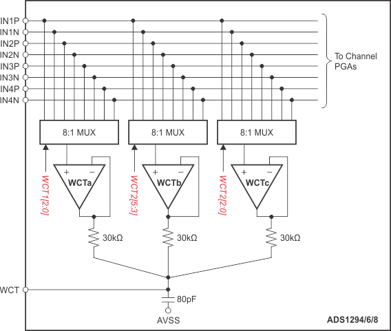 Figure 35. WCT Voltage
These devices provide the flexibility to route any one of the eight signals (IN1P to IN4N) to each of the amplifiers to generate the average. This flexibility allows the RA, LA, and LL electrodes to be connected to any input of the first four channels, depending on the lead configuration.
Each of the three amplifiers in the WCT circuitry can be powered down individually with register settings. By powering up two amplifiers, the average of any two electrodes is generated at the WCT pin. Powering up one amplifier provides the buffered electrode voltage at the WCT pin. The WCT amplifiers have limited drive strength, and thus, should be buffered if used to drive a low-impedance load.
Table 6 shows the typical WCT performance when using any 1, 2, or 3 of the WCT buffers.
Table 6. Typical WCT Performance
| PARAMETER | ANY ONE (A, B, or C) |
ANY TWO (A+B, A+C, or B+C) |
ALL THREE (A+B+C) |
UNIT |
|---|---|---|---|---|
| Integrated noise | 540 | 382 | 312 | nVRMS |
| Power | 53 | 59 | 65 | μW |
| –3-dB BW | 30 | 59 | 89 | kHz |
| Slew rate | BW limited | BW limited | BW limited | V/μs |
As shown in Table 6, the overall noise reduces when more than one WCT amplifier is powered up. This noise reduction is a result of the fact that noise is averaged by the passive summing network at the output of the amplifiers. Powering down individual buffers gives negligible power savings because a significant portion of the circuitry is shared between the three amplifiers. The bandwidth of the WCT node is limited by the RC network. The internal summing network consists of three 30-kΩ resistors and a 80-pF capacitor. For optimal performance, add an external 100-pF capacitor. The effective bandwidth depends on the number of amplifiers that are powered up, as shown in Table 6.
Only use the WCT node to drive very high input impedances (typically greater than 500 MΩ). A typical application connects this WCT signal to the negative inputs of a ADS129x for use as a reference signal for the chest leads.
As mentioned, all three WCT amplifiers can be connected to one of eight analog input pins. The inputs of the amplifiers are chopped, and the chop frequency varies with the data rates of the ADS129x. The chop frequency for the three highest data rates scale 1:1. For example, at a 32-kSPS data rate, the chop frequency is 32 kHz in HR mode with WCT_CHOP = 0. The chop frequency of the four lower data rates is fixed at 4 kHz. When WCT_CHOP = 1, the chop frequency is fixed to highest data rate frequency (that is, fMOD / 16), as shown in Table 7. The chop frequency appears at the output of the WCT amplifiers as a small square wave riding on dc. The amplitude of the square wave is the offset of the amplifier and is typically 5 mVPP. As a result of out-of-band chopping, this artifact does not interfere with ECG-related measurements. As a result of the chopping function, the input current leakage on the pins with the connected WCT amplifiers increases at higher data rates and as the input common voltage swings closer to 0 V (AVSS), as described in Figure 36.
If the output of a channel connected to the WCT amplifier (for example, the V-lead channels) is connected to one of the pace amplifiers for external pace detection, the chopping artifact appears at the pace amplifier output.
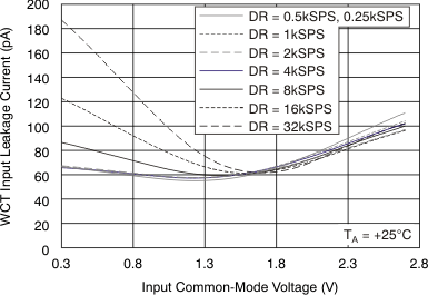 Figure 36. WCT Input Leakage Current vs Input Voltage (WCT_CHOP = 0)
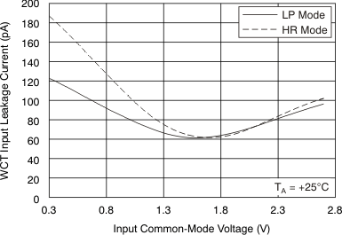 Figure 37. WCT Input Leakage Current vs Input Voltage (WCT_CHOP = 1)
Table 7. WCT Amplifiers Chop Frequency
| CONFIG1.DR[2:0] BIT | CONFIG2.WCT_CHOP = 0 | CONFIG2.WCT_CHOP = 1 |
|---|---|---|
| 000 | fMOD/16 | fMOD/16 |
| 001 | fMOD / 32 | fMOD / 16 |
| 010 | fMOD / 64 | fMOD / 16 |
| 011 | fMOD / 128 | fMOD / 16 |
| 100 | fMOD / 128 | fMOD / 16 |
| 101 | fMOD / 128 | fMOD / 16 |
| 110 | fMOD / 128 | fMOD / 16 |
9.3.1.7.3.1 Augmented Leads
In a typical implementation of the 12-lead ECG with eight channels, the augmented leads are calculated digitally. In certain applications, it may be required that all leads are derived in analog rather than digital. The ADS1298 and ADS1298R provide the option to generate the augmented leads by routing appropriate averages to channels 5, 6, and 7. The same three amplifiers that are used to generate the WCT signal are also used to generate the Goldberger central terminal (GCT) signals. Figure 38 shows an example of generating the augmented leads in analog domain. In this implementation, more than eight channels are used to generate the standard 12 leads. This feature is not available in the ADS1294, ADS1294R, ADS1296 and ADS1296R.
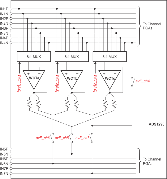 Figure 38. Analog Domain Augmented Leads
9.3.1.7.3.2 Right Leg Drive with the WCT Point
In certain applications, the out-of-phase version of the WCT is used as the RLD reference. The ADS1298 provides the option to have a buffered version of the WCT terminal at the RLD_OUT pin. This signal can be inverted in phase using an external amplifier and then used as the right leg drive. Refer to the Right Leg Drive (RLD DC Bias Circuit) section for more details.
9.3.1.7.4 Lead-Off Detection
Patient electrode impedances decay over time; therefore, these electrode connections must be continuously monitored to verify that a suitable connection is present. The ADS129x lead-off detection functional block provides significant flexibility to choose from various lead-off detection strategies. Although called lead-off detection, this feature is in fact electrode-off detection.
The basic principle is to inject an excitation signal and measure the response to determine if the electrode is off. As shown in the lead-off detection functional block diagram in Figure 39, this circuit provides two different methods of determining the state of the patient electrode. The methods differ in the frequency content of the excitation signal. Lead-off can be selectively done on a per channel basis using the LOFF_SENSP and LOFF_SENSN registers. The internal excitation circuitry can be disabled while the sensing circuitry is enabled.
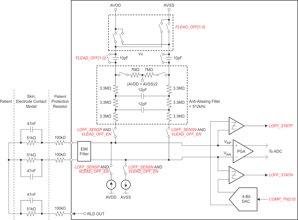 Figure 39. Lead-Off Detection
9.3.1.7.4.1 DC Lead-Off
In this approach, the lead-off excitation is accomplished with a dc signal. Choose a dc excitation signal from either a pullup or pulldown resistor, or from a current source or sink system, as shown in Figure 40. Select by setting the VLEAD_OFF_EN bit in the LOFF register. One side of the channel is pulled to supply, and the other side is pulled to ground. Swap the pullup resistor and pulldown resistor by setting the bits in the LOFF_FLIP register, as shown in Figure 41. If using a current source or sink, set the magnitude of the current by using the ILEAD_OFF[1:0] bits in the LOFF register. The current source or sink gives larger input impedance compared to the 10-MΩ pullup or pulldown resistor.
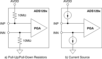 Figure 40. DC Lead-Off Excitation Options
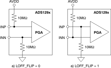 Figure 41. LOFF_FLIP Usage
Response sensing is achieved either by looking at the digital output code from the device, or by monitoring the input voltages with on-chip comparators. If either of the electrodes is off, the pullup or pulldown resistors saturate the channel. Look at the output code to determine if either the P-side or the N-side is off. To pinpoint which side is off, check the comparator outputs. During conversion, the input voltage is simultaneously monitored by using a comparator and a 4-bit DAC with levels that are set by the COMP_TH[2:0] bits in the LOFF register. The comparator outputs are stored in the LOFF_STATP and LOFF_STATN registers. These two registers are available as a part of the output data stream (see the Data Output Pin (DOUT) section). If dc lead-off is not used, the lead-off comparators can be powered down by setting the PD_LOFF_COMP bit in the CONFIG4 register.
An example procedure to turn on dc lead-off is given in the Lead-Off section.
9.3.1.7.4.2 AC Lead-Off
This method uses an out-of-band ac signal for excitation. The ac signal is generated by providing pullup and pulldown resistors at the input with a fixed frequency. The ac signal is passed through an antialiasing filter to prevent aliasing. Select the frequency with the FLEAD_OFF[1:0] bits in the LOFF register. The excitation frequency is a function of the output data rate and is fDR / 4. This out-of-band excitation signal is passed through the channel and measured at the output.
AC signal sensing is achieved by passing the signal through the channel to digitize the signal, and measuring the output. The ac excitation signals are introduced at a frequency that is above the band of interest, generating an out-of-band differential signal that can be filtered out separately and processed. By measuring the magnitude of the excitation signal at the output spectrum, the lead-off status is calculated. Therefore, the ac lead-off detection is accomplished simultaneously with the ECG signal acquisition.
9.3.1.7.5 RLD Lead-Off
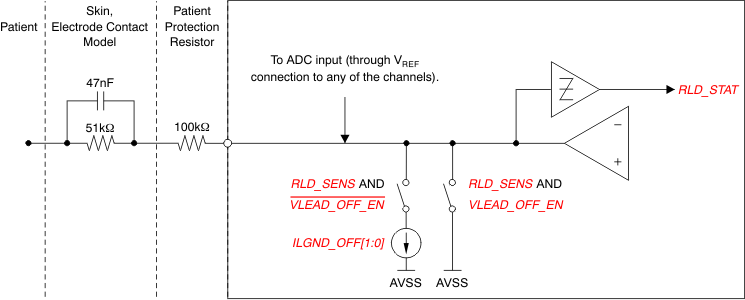
Determine if the RLD electrode is connected in the ADS129x by powering down the RLD amplifier. After power down, there are two measurement procedures to determine the RLD electrode connect status: a pullup or pulldown resistor, or a sink or source current source, as shown in Figure 42. Set the reference level of the comparator to determine the acceptable RLD impedance threshold.
The current source, or pullup or pulldown resistor method has no function when the RLD amplifier is powered on. Use the comparator to sense the voltage at the output of the RLD amplifier. The comparator threshold is set by the same LOFF[7:5] bits that are used to set the thresholds for the other negative inputs.
9.3.1.7.6 Right Leg Drive (RLD) DC Bias Circuit
Use the right leg drive (RLD) circuitry to counter the common-mode interference in a ECG system as a result of power lines and other sources, including fluorescent lights. The RLD circuit senses the common-mode voltage of a selected set of electrodes and creates a negative feedback loop by driving the body with an inverted common-mode signal. The negative feedback loop restricts the common-mode movement to a narrow range, depending on the loop gain. Stabilizing the entire loop is specific to the individual system, based on the various poles in the loop. The ADS129x incorporate muxes that are used to select the channel to the operational amplifier. All the amplifier terminals are available at the pins, allowing selection of the components for the feedback loop. The circuit shown in Figure 43 shows the overall functional connectivity for the RLD bias circuit.
Set the reference voltage for the RLD to be generated internally ([AVDD + AVSS] / 2), or provided externally with a resistive divider. The selection of an internal versus external reference voltage for the RLD loop is defined by writing the appropriate value to the RLDREF_INT bit in the CONFIG3 register.
If the RLD function is not used, power down the amplifier using the PD_RLD bit (see the CONFIG3: Configuration Register 3 (address = 03h) (reset = 40h) section for details). This bit is also used in daisy-chain mode to power down all but one of the RLD amplifiers.
The functionality of the RLDIN pin is explained in the Input Multiplexer section. An example procedure to use the RLD amplifier is shown in the Right Leg Drive section of the Power-Supply Recommendations.
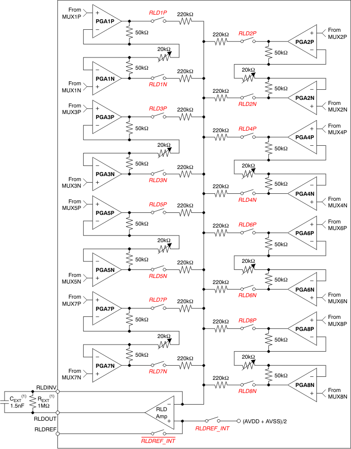
9.3.1.7.6.1 WCT as RLD
In certain applications, the RLD is derived as the average of RA, LA, and LL. This level is the same as the WCT voltage. The WCT amplifier has limited drive strength; therefore, only use the WCT to drive very high impedances directly. The ADS129x provide an option to internally buffer the WCT signal by setting the WCT_TO_RLD bit in the CONFIG4 register. Short the RLD_OUT and RLD_INV pins external to the device. Before the RLD_OUT signal is connected to the RLD electrode, use an external amplifier to invert the phase of the signal for negative feedback.
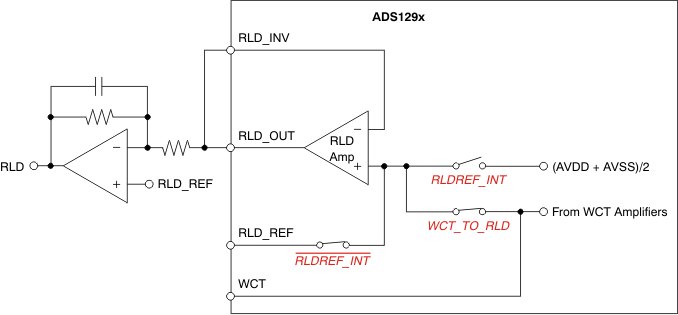 Figure 44. Using the WCT as the Right Leg Drive (RLD)
9.3.1.7.6.2 RLD Configuration with Multiple Devices
Figure 45 shows multiple devices connected to an RLD.
 Figure 45. RLD Connection for Multiple Devices
9.3.1.7.7 Pace Detect
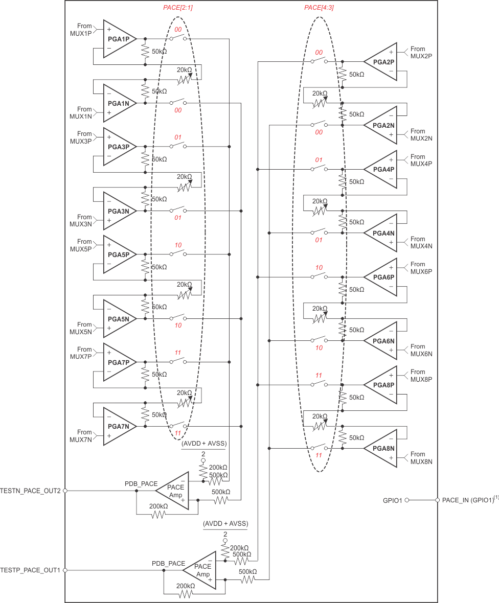
The ADS129x provide flexibility for pace detection by using either software or external hardware. The software approach is made possible by providing sampling rates up to 32 kSPS. The external hardware approach is made possible by bringing out the output of the PGA at two pins: TESTP_PACE_OUT1 and TESTN_PACE_OUT2. If the WCT amplifier is connected to the signal path, switching noise occurs as a result of chopping; see the Wilson Central Terminal (WCT) and Chest Leads section for details.
9.3.1.7.7.1 Software Approach
To use the software approach, operate the device at 8 kSPS or more to capture the fastest pulse. Afterwards, digital signal processing is used to identify the presence of the pacemaker pulse. The software approach gives the utmost flexibility to program the pace detect threshold on-the-fly (dynamically) using software. This flexibility is increasingly important as pacemakers evolve over time. Two parameters must be considered while measuring fast pace pulses:
- PGA bandwidth: determines the gain setting that can be used; shown in Table 5.
- Settling time: determines the operating data rate for the device. For a step change in input, the digital decimation filter takes 3 × tDR to settle.
9.3.1.7.7.2 External Hardware Approach
One of the drawbacks of using the software approach is that all channels on a single device must operate at higher data rates. For systems where high data rates are a problem, the ADS129x provide the option of connecting external hardware to the output of the PGA to detect the presence of the pulse. The output of the pace detection logic is then fed into the device through one of the GPIO pins. The GPIO data are transmitted through the SPI port and loaded 2 tCLKs before DRDY goes low. Two of the eight channels are selected using register bits in the PACE register: one from the odd-numbered channels, and the other from the even-numbered channels. During the differential to single-ended conversion, there is an attenuation of 0.4; therefore, the total gain in the pace path is equal to (0.4 × PGA_GAIN). The pace output signals are multiplexed with the TESTP and TESTN signals through the TESTP_PACE_OUT1 and TESTN_PACE_OUT2 pins, respectively. Channel selection is achieved by setting bits[4:1] of the PACE register. If the pace circuitry is not used, turn off the pace amplifiers by using the PD_PACE bit in the PACE register.
If the output of a channel connected to the WCT amplifier (for example, the V-lead channels) is connected to one of the pace amplifiers for external pace detection, chopping artifacts appear at the pace amplifier output. See the Wilson Central Terminal (WCT) and Chest Leads section for more details.
9.3.1.7.8 Respiration
As shown in Table 8, the ADS129xR provide three options for respiration impedance measurement: external respiration, internal respiration using on-chip modulation signals, and internal respiration using user-generated modulation signals. The ADS129x provides only external respiration impedance measurement.
Table 8. Respiration Control
| RESP.RESP_CTRL[1] | RESP.RESP_CTRL[0] | DESCRIPTION | MODE AVAILABLE |
|---|---|---|---|
| 0 | 0 | Respiration disabled | ADS129x, ADS129xR |
| 0 | 1 | Generates modulation and demodulation signals for external respiration circuitry. RESP_CLK signals on GPIO2, GPIO3, and GPIO4. | ADS129x, ADS129xR |
| 1 | 0 | Respiration measurement using internally-generated RESP_MOD signals. | ADS129xR |
| 1 | 1 | Respiration measurement using user-generated modulation and blocking signal. | ADS129xR(1) |
For more information on respiration impedance measurement, see Respiration Rate Measurement Using Impedance Pneumography, SBAA181.
9.3.1.7.8.1 External Respiration Circuitry (RESP_CTRL = 01b)
With this option, GPIO2, GPIO3, and GPIO4 are automatically configured as outputs. The phase relationship between the signals is shown in Figure 47. GPIO2 is the exclusive-OR of GPIO3 and GPIO4, as shown in Figure 48. GPIO3 is the modulation signal, and GPIO4 is the demodulation signal. While using this option, the general-purpose pin functions of GPIO2, GPIO3, and GPIO4 are not available. The modulation frequency is set to either 64 kHz or 32 kHz by using the RESP_FREQ[2:0] bits in the CONFIG4 register. The remaining bit options of RESP_FREQ[2:0] generate square waves on GPIO3 and GPIO4. The exclusive-OR out on GPIO2 is only available in 64-kHz or 32-kHz. The phase of GPIO4, relative to GPIO3, is set by RESP_PH[2:0] bits in the RESP register.
Use this option to implement custom respiration impedance circuitry external to the ADS129x.

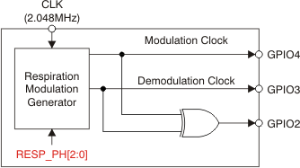 Figure 48. External Respiration (RESP_CTRL = 01b) Block Diagram
Table 9. Switching Characteristics for Figure 47(1)
| PARAMETER | 2.7 V ≤ DVDD ≤ 3.6 V | 1.65 V ≤ DVDD ≤ 2 V | UNIT | |||||
|---|---|---|---|---|---|---|---|---|
| MIN | TYP | MAX | MIN | TYP | MAX | |||
| tPHASE | Respiration phase delay, set by RESP.RESP_PH[2:0] | 22.5 | 157.5 | 22.5 | 157.5 | Degrees | ||
| tBLKDLY | Modulation clock rising edge to XOR signal | 1 | 5 | ns | ||||
9.3.1.7.8.2 Internal Respiration Circuitry with Internal Clock (RESP_CTRL = 10b, ADS129xR Only)
Figure 49 shows a block diagram of the internal respiration circuitry. The internal modulation and demodulator circuitry can be selectively used.
The modulation block is controlled by the RESP_MOD_EN bit and the demodulation block is controlled by the RESP_DEMOD_EN bit. The modulation signal is a square wave of magnitude VREFP – AVSS. Using this option, the output of the modulation circuitry is available at the RESP_MODP and RESP_MODN pins of the device. This availability allows custom filtering to be added to the square-wave modulation signal. Using this option, GPIO2, GPIO3, and GPIO4 can be used for other purposes. The modulation frequency is either 64 kHz or 32 kHz, as set by the RESP_FREQ[2:0] bits in the CONFIG4 register. The phase of the internal demodulation signal is set by the RESP_PH[2:0] bits in the RESP register.
When this respiration option is enabled, ADS129xR channel 1 cannot be used to acquire ECG signals. If the RA and LA leads are intended to measure respiration and ECG signals, wire the two leads into channel 1 for respiration and channel 2 for ECG signals.
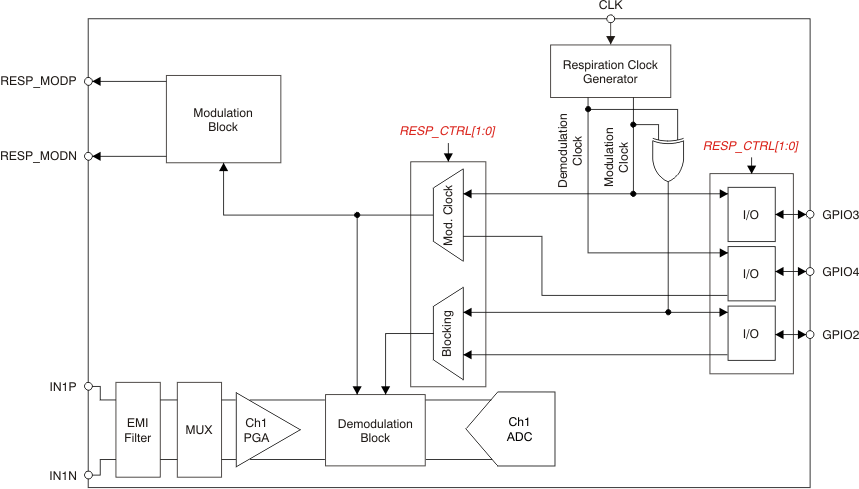 Figure 49. Internal Respiration Block Diagram
9.3.1.7.8.3 Internal Respiration Circuitry With User-Generated Signals (RESP_CTRL = 11b, ADS129xR Only)
In this mode GPIO2, GPIO3, and GPIO4 are automatically configured as inputs and cannot be used for other purposes. The signals must be provided as described in Figure 50. Do not use the internal master clock in this mode.
 Figure 50. Internal Respiration (RESP_CTRL = 11b) Timing Diagram
9.3.2 Digital Functionality
9.3.2.1 GPIO Pins (GPIO[4:1])
The ADS129x have a total of four general-purpose digital input/output (GPIO) pins available in normal operation. The digital I/O pins are individually configurable as either inputs or as outputs through the GPIOC bits of the GPIO register. The GPIOD bits in the GPIO register control the level of the pins. When reading the GPIOD bits, the data returned are the logic level of the pins, whether they are programmed as inputs or outputs. When the GPIO pin is configured as an input, a write to the corresponding GPIOD bit has no effect. When configured as an output, a write to the GPIOD bit sets the output value.
If configured as inputs, these pins must be driven; do not float these pins. The GPIO pins are set as inputs after power-on or after a reset. Figure 51 shows the GPIO port structure. If not used, short these pins to DGND.
For example, one configuration is to use GPIO1 as the PACEIN signal, multiplex GPIO2 with RESP_BLK signal, multiplex GPIO3 with the RESP signal, and multiplex GPIO4 with the RESP_PH signal.
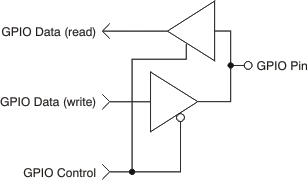 Figure 51. GPIO Port Pin
9.3.2.2 Power-Down Pin (PWDN)
When PWDN is pulled low, all on-chip circuitry is powered down. To exit power-down mode, take the PWDN pin high. Upon exiting from power-down mode, the internal oscillator and the reference require time to wakeup. During power down, shut down the external clock to save power.
9.3.2.3 Reset (RESET Pin and Reset Command)
There are two methods to reset the ADS129x: pull the RESET pin low, or send the RESET opcode command (see the RESET: Reset Registers to Default Values section). Take the RESET pin low to force a reset. Make sure to follow the minimum pulse width timing specifications before taking the RESET pin back high. The RESET command takes effect on the eighth SCLK falling edge of the opcode command. At reset, 18 tCLK cycles are required to complete initialization of the configuration registers to the default states and start the conversion cycle. For more information, see the RESET: Reset Registers to Default Values section. An internal reset is automatically issued to the digital filter whenever registers CONFIG1 and RESP are set to new values with a WREG command.
9.3.2.4 Digital Decimation Filter
The digital filter receives the modulator output and decimates the data stream. By adjusting the amount of filtering, tradeoffs are made between resolution and data rate: filter more for higher resolution, filter less for higher data rates. Higher data rates are typically used in ECG applications to implement software pace detection and ac lead-off detection.
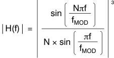
The digital filter on each channel consists of a third-order sinc filter. The decimation ratio on the sinc filters is adjusted by the DR bits in the CONFIG1 register (see Table 16 for details). This setting is a global setting that affects all channels; therefore, in these devices, all channels operate at the same data rate.
9.3.2.4.1 Sinc Filter Stage (sinx / x)
The sinc filter is a variable-decimation rate, third-order, low-pass filter. Data are supplied to this section of the filter from the modulator at the rate of fMOD. The sinc filter attenuates the high-frequency noise of the modulator, then decimates the data stream into parallel data. The decimation rate affects the overall data rate of the converter.
Equation 4 shows the scaled Z-domain transfer function of the sinc filter.

The frequency-domain transfer function of the sinc filter is shown in Equation 5.
The sinc filter has notches (or zeroes) that occur at the output data rate multiples. At these frequencies, the filter has infinite attenuation. Figure 52 shows the frequency response of the sinc filter and Figure 53 shows the rolloff of the sinc filter. With a step change at input, the filter requires 3 × tDR conversion cycles to settle. After a rising edge of the START pin or completion of the START command, the filter takes tSETTLE periods to give the first data output. The settling time of the filters at various data rates are discussed in the Start Mode subsection of the SPI Interface section. Figure 54 and Figure 55 show the filter transfer function to fMOD / 2 and fMOD / 16, respectively, at different data rates. Figure 56 shows the transfer function extended out to 4 × fMOD. As shown in the figures, the passband of the ADS129x repeats itself at every fMOD muiltple. Choose input R-C antialiasing filters for the system that sufficiently attenuate any interference in frequencies around multiples of fMOD.
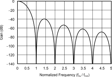 Figure 52. Sinc Filter Frequency Response
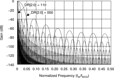 Figure 54. Transfer Function of On-Chip Decimation Filters to fMOD / 2
![ADS1294 ADS1294R ADS1296 ADS1296R ADS1298 ADS1298R Transfer
Function of On-Chip Decimation Filters
to 4 × fMOD for DR[2:0] = 000 and DR[2:0] = 110 ADS1294 ADS1294R ADS1296 ADS1296R ADS1298 ADS1298R ai_tx_funct_bas459.gif](/ods/images/SBAS459K/ai_tx_funct_bas459.gif) Figure 56. Transfer Function of On-Chip Decimation Filters
Figure 56. Transfer Function of On-Chip Decimation Filtersto 4 × fMOD for DR[2:0] = 000 and DR[2:0] = 110
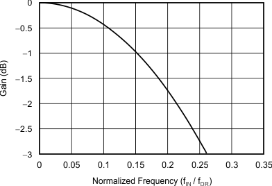 Figure 53. Sinc Filter Roll-Off
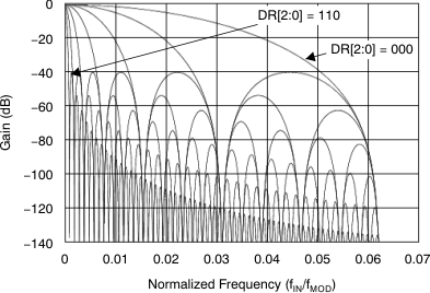 Figure 55. Transfer Function of On-Chip Decimation Filters to fMOD / 16
9.3.2.5 Clock
The ADS129x provide two different methods for device clocking: internal and external. Internal clocking is ideally suited for low-power, battery-powered systems. The internal oscillator is trimmed for accuracy at room temperature. The accuracy varies over the specified temperature range; see the Electrical Characteristics. Clock selection is controlled by the CLKSEL pin and the CLK_EN register bit.
Use the CLKSEL pin to select either the internal or external clock. The CLK_EN bit in the CONFIG1 register enables and disables the oscillator clock to be output in the CLK pin. A truth table for these two pins is shown in Table 11. Use the CLK_EN bit is when multiple devices are connected in a daisy-chain configuration. During power down, shut down the external clock to save power.
Table 11. CLKSEL Pin and CLK_EN Bit
| CLKSEL PIN | CONFIG1.CLK_EN BIT | CLOCK SOURCE | CLK PIN STATUS |
|---|---|---|---|
| 0 | X | External clock | Input: external clock |
| 1 | 0 | Internal clock oscillator | Tri-state |
| 1 | 1 | Internal clock oscillator | Output: internal clock oscillator |
9.4 Device Functional Modes
9.4.1 Data Acquisition
This section describes the data acquisition process in relation to the START and DRDY pins, settled data, and data readback.
9.4.1.1 Start Mode
Pull the START pin high for at least 2 tCLK periods, or send the START command to begin conversions. When the START pin is low, or if the START command has not been sent, the device does not issue a DRDY signal (conversions are halted).
When using the START opcode to begin conversions, hold the START pin low. The ADS129x feature two modes to control conversion: continous and single-shot. The mode is selected by SINGLE_SHOT (bit 3 of the CONFIG4 register). In multiple device configurations, the START pin is used to synchronize devices (see the Multiple-Device Configurationsection for more details).
9.4.1.1.1 Settling Time
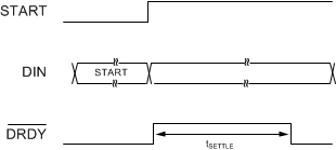
The settling time (tSETTLE) is the time it takes for the converter to output fully-settled data when the START signal is pulled high.
When the START pin is pulled high, or when the START command is sent, the device ADCs convert the input signals and DRDY is pulled high. The next falling edge of DRDY indicates that data are ready. Figure 57 shows the timing diagram and Table 12 shows the settling time for different data rates as a function of tCLK. The settling time depends on fCLK and the decimation ratio (controlled by the DR[2:0] bits in the CONFIG1 register).
Table 12. Settling Times for Different Data Rates (tSETTLE)
| DR[2:0] | SETTLING TIME (tCLK Periods) | |
|---|---|---|
| HIGH-RESOLUTION MODE | LOW-POWER MODE | |
| 000 | 296 | 584 |
| 001 | 584 | 1160 |
| 010 | 1160 | 2312 |
| 011 | 2312 | 4616 |
| 100 | 4616 | 9224 |
| 101 | 9224 | 18440 |
| 110 | 18440 | 36872 |
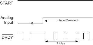
When the START pin is held high and there is a step change in the input signal, 3 × tDR conversion cycles are required for the filter to settle to the new value, as shown in Figure 58. Settled data are available on the fourth DRDY pulse. This settling time must be considered when trying to measure narrow pace pulses for pace detection. Data are available to read at each DRDY high-to-low transition, but can be ignored.
9.4.1.2 Data Ready Pin (DRDY)
DRDY is an output. When DRDY transitions low, new conversion data are ready. The CS signal has no effect on the data ready signal. Regardless of the status of the CS signal, a rising edge on SCLK pulls DRDY high. Thus, when using multiple devices in the SPI bus, gate SCLK with CS. The behavior of DRDY depends on if the device is in RDATAC mode or if the RDATA command is being used to read data on demand. See the RDATAC: Read Data Continuous and RDATA: Read Datasections for further details.
When reading data with the RDATA command, the read operation can overlap the occurrence of the next DRDY without data corruption.
Use the START pin or the START command to place the device either in normal data capture mode or pulse data capture mode.
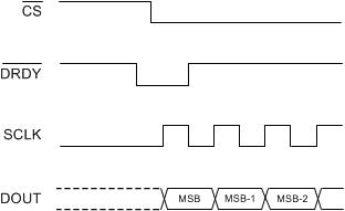
Figure 59 shows the relationship among DRDY, DOUT, and SCLK during data retrieval (in the case of an ADS129x with a selected data rate that gives 24-bit resolution). DOUT latches at the rising edge of SCLK. The device pulls DRDY high at the first falling edge of SCLK, regardless of whether data are being retrieved from the device or a command is being sent through the DIN pin. The data starts from the MSB of the status word and then proceeds to the ADC channel data in sequential order (that is, channel 1, channel 2, ..., channel x). Channels that are powered down still have a position in the data stream; however, the data are not valid and can be ignored.
The DRDY signal is cleared on the first SCLK falling edge, regardless of the state of CS. Even if no data are clocked out, the DRDY signal is still cleared. Take this condition into consideration if the SPI bus is used to communicate with other devices on the same bus. Figure 60 shows a timing diagram for this multiplexing.
9.4.1.3 Data Retrieval
Data retrieval is accomplished in one of two methods:
- RDATAC: the read data continuous command sets the device mode that reads data continuously without sending opcodes. See the RDATAC: Read Data Continuous section for more details.
- RDATA: the read data command reads just one data output from the device. See the RDATA: Read Data section for more details.
The conversion data are read by shifting the data out on DOUT. The MSB of the data on DOUT is clocked out on the first SCLK rising edge. DRDY returns to high on the first SCLK falling edge. Keep DIN low for the entire read operation.
9.4.1.3.1 Status Word
The ADS129x data readback is preceded by a status word that provides information on the state of the ADC. The status word is 24 bits long and contains the values for LOFF_STATP, LOFF_STATN, and part of the GPIO registers. The content alignment is shown in Figure 61.
 Figure 61. Status Word Content
9.4.1.3.2 Readback Length
The number of bits in the data output depends on the number of channels and the number of bits per channel. The data format for each channel data is twos complement and MSB first. For the ADS129x with 32-kSPS and 64-kSPS data rates, the number of data bits is 24 status bits + 16 bits per channel × 8 channels = 152 bits. For all other data rates, the number of data bits is 24 status bits + 24 bits per channel × 8 channels = 216 bits. When channels are powered down using the user-register setting, the corresponding channel output is set to 0. However, the sequence of channel outputs remains the same. The ADS1294 outputs four channels of datam and the ADS1296 outputs six channels of data.
The ADS129x also provide a multiple-readback feature. Set the DAISY_IN bit in the CONFIG1 register to 1 for multiple readbacks. Simply provide additional SCLKs to read data multiple times; the MSB data byte repeats after reading the last byte.
9.4.1.3.3 Data Format
The ADS129x output 24 bits of data per channel in binary twos complement format, MSB first. The LSB has a weight of VREF / (223 – 1). A positive full-scale input produces an output code of 7FFFFFh and the negative full-scale input produces an output code of 800000h. The output clips at these codes for signals exceeding full-scale. Table 13 summarizes the ideal output codes for different input signals. For DR[2:0] = 000 and 001, the device has only 17 and 19 bits of resolution, respectively. The last seven (in 17-bit mode) or five (in 19-bit mode) bits can be ignored.
Table 13. Ideal Output Code versus Input Signal(1)
| INPUT SIGNAL, VIN
(INxP – INxN) |
IDEAL OUTPUT CODE(2) |
|---|---|
| ≥ VREF | 7FFFFFh |
| VREF / (223 – 1) | 000001h |
| 0 | 000000h |
| –VREF / (223 – 1) | FFFFFFh |
| ≤ –VREF (223 / (223 – 1)) | 800000h |
9.4.1.4 Single-Shot Mode
Enable single-shot mode by setting the SINGLE_SHOT bit in CONFIG4 register to 1. In single-shot mode, the ADS129x perform a single conversion when the START pin is taken high, or when the START opcode command is sent. As seen in Figure 62, when a conversion completes, DRDY goes low and further conversions are stopped. Regardless of whether the conversion data are read or not, DRDY remains low. To begin a new conversion, take the START pin low and then back high for at least two tCLKs, or transmit the START opcode again. When switching from continous conversion mode to single-shot mode, make sure the START signal is pulsed, or issue a STOP command followed by a START command.
 Figure 62. DRDY With No Data Retrieval in Single-Shot Mode
Single-shot conversion mode is provided for applications that require nonstandard or noncontinuous data rates. Issue a START command or toggle the START pin high to reset the digital filter, effectively dropping the data rate by a factor of four. This mode leaves the system more susceptible to aliasing effects, thus requiring more complex analog or digital filtering. Loading on the host processor increases because it must toggle the START pin or send a START command to initiate a new conversion cycle.
9.4.1.5 Continuous Conversion Mode
Conversions begin when the START pin is taken high for at least two tCLKs, or when the START opcode command is sent. As seen in Figure 63, the DRDY output goes high when conversions are started and goes low when data are ready. Conversions continue indefinitely until the START pin is taken low or the STOP opcode command is transmitted. When the START pin is pulled low or the stop command is issued, the conversion in progress is allowed to complete. Figure 64 and Table 14 show the required timing of DRDY to the START pin and the START and STOP opcode commands when controlling conversions in this mode. To keep the converter running continuously, permanently tie the START pin high. When switching from single-shot mode to continous-conversion mode, pulse the START signal or a issue a STOP command followed by a START command. This conversion mode is ideal for applications that require a continuous stream of conversions results.
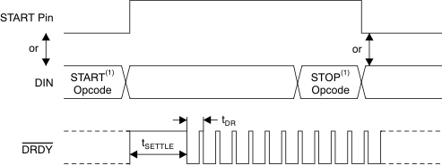
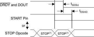
Table 14. Timing Requirements for Figure 64(1)
| MIN | MAX | UNIT | ||
|---|---|---|---|---|
| tSDSU | START pin low or STOP opcode to DRDY setup time to halt further conversions | 16 | tCLK | |
| tDSHD | START pin low or STOP opcode to complete current conversion | 16 | tCLK | |
9.4.2 Multiple-Device Configuration
The ADS129x provide configuration flexibility when multiple devices are connected in a system. The serial interface typically requires four signals: DIN, DOUT, SCLK, and CS. With one additional chip select signal per device, multiple devices can be connected together. The number of signals required to interface n devices is 3 + n.
Daisy-chain the RLD amplifiers as explained in the RLD Configuration with Multiple Devices section. To use the internal oscillator in a daisy-chain configuration, set one of the devices as the master for the clock source with the internal oscillator enabled (CLKSEL pin = 1) and the internal oscillator clock brought out of the device by setting the CLK_EN register bit to 1. Use this master device clock as the external clock source for the other devices.
When using multiple devices, synchronize the devices with the START signal. The delay from the START signal to the DRDY signal is fixed for a fixed data rate (see the Start Mode section for more details on the settling times). As an example, Figure 65 shows the behavior of two devices when synchronized with the START signal.
There are two configurations used to connect multiple devices with a optimal number of interface pins: cascade or daisy-chain.
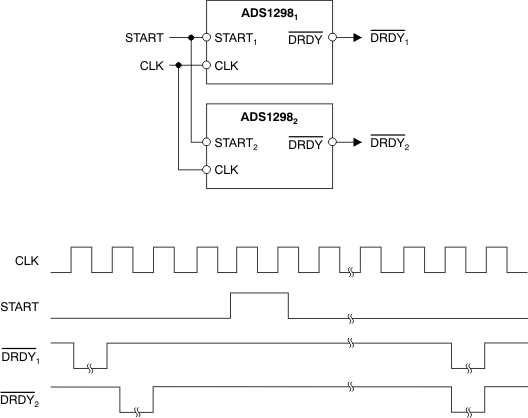 Figure 65. Synchronizing Multiple Converters
9.4.2.1 Cascade Configuration
Figure 66(a) shows a configuration with two devices cascaded together. One of the devices is an ADS1298 (eight channels) and the other is an ADS1294 (four channels). Together, they create a system with 12 channels. DOUT, SCLK, and DIN are shared. Each device has its own chip select. When a device is not selected by the corresponding CS being driven to logic 1, the DOUT of this device is high-impedance. This structure allows the other device to take control of the DOUT bus. This configuration method is suitable for the majority of applications.
9.4.2.2 Daisy-Chain Configuration
Enable daisy-chain mode by setting the DAISY_EN bit in the CONFIG1 register. Figure 66(b) shows the daisy-chain configuration. In this configuration, SCLK, DIN, and CS are shared across multiple devices. Connect the DOUT pin of the first device to the DAISY_IN pin of the next device, thereby creating a chain. Issue one extra SCLK between each data set. Note that when using daisy-chain mode, the multiple readback feature is not available. Short the DAISY_IN pin to digital ground if not used. Figure 2 describes the required timing for the ADS1298 shown in Figure 67. Data from the ADS1298 appear first on DOUT, followed by a don’t care bit, and finally by the status and data words from the ADS1294.
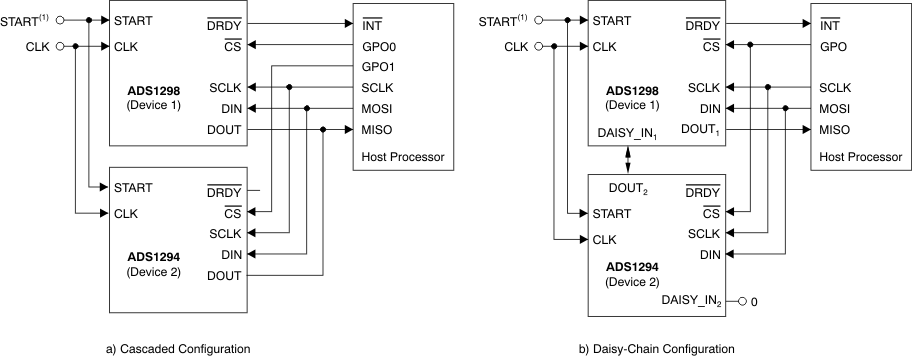
Important reminders when using daisy-chain mode:
- Issue one extra SCLK between each data set (see Figure 67).
- All devices are configured to the same register values because CS is shared.
- Device register readback (RREG) is only valid for device 0 in the daisy chain. Only conversion data can be read from device 1 to device N, where N is the last device in the chain; register data cannot be read.
If all devices in the chain operate in the same register setting, DIN can be shared, thereby reducing the SPI communication signals to four, regardless of the number of devices. However, the individual devices cannot be programmed; therefore, the RLD driver cannot be shared among the multiple devices. Furthermore, an external clock must be used.
As shown in Figure 2, the SCLK rising edge shifts data out of the ADS129x on DOUT. The SCLK rising edge is also used to latch data into the device DAISY_IN pin down the chain. This architecture allows for a faster SCLK rate speed, but it also makes the interface sensitive to board-level signal delays. The more devices in the chain, the more challenging it becomes to adhere to setup and hold times. A star-pattern connection of SCLK to all devices, minimizing length of DOUT, and other PCB layout techniques help. Placing delay circuits such as buffers between DOUT and DAISY_IN is another way to mitigate this challenge. One other option is to insert a D flip-flop between DOUT and DAISY_IN clocked on an inverted SCLK. In addition, note that daisy-chain mode requires some software overhead to recombine data bits spread across byte boundaries.
The maximum number of daisy-chained devices depends on the data rate at which the device is operated. The maximum number of devices can be estimated with Equation 6:

where
- NBITS = device resolution (depends on data rate)
- NCHANNELS = number of channels in the device (4, 6, or 8)
For example, when the ADS1298 (eight-channel, 24-bit version) is operated at a 2-kSPS data rate with a 4-MHz fSCLK, up to ten devices can be daisy-chained.
9.5 Programming
9.5.1 SPI Interface
The SPI-compatible serial interface consists of four signals: CS, SCLK, DIN, and DOUT. The interface reads conversion data, reads and writes registers, and controls the ADS129x operation. The DRDY output is used as a status signal to indicate when data are ready. DRDY goes low when new data are available.
9.5.1.1 Chip Select Pin (CS)
Chip select (CS) selects the ADS129x devices for SPI communication. While CS is low, the serial interface is active. CS must remain low for the entire duration of the serial communication. After the serial communication is finished, always wait four or more tCLK periods before taking CS high. When CS is taken high, the serial interface resets, SCLK and DIN are ignored, and DOUT enters a high-impedance state. DRDY asserts when data conversion is complete, regardless of whether CS is high or low.
While ADS129x is selected, the device attempts to decode and execute commands every eight serial clocks. If the device ceases to execute serial commands, it is possible extra clock pulses were presented that placed the serial interface into an unknown state. To reset the serial interface to a known state, take CS high and back low again.
9.5.1.2 Serial Clock (SCLK)
SCLK is the serial peripheral interface (SPI) serial clock. It is used to shift in commands and shift out data from the device. The serial clock (SCLK) features a Schmitt-triggered input, and clocks data on the DIN and DOUT pins into and out of the ADS129x. Even though the input has hysteresis, keep SCLK as clean as possible to prevent glitches from accidentally forcing a clock event. The absolute maximum limit for SCLK is specified in the Timing Requirements: Serial Interface table.
While ADS129x is selected (CS = low), the device attempts to decode and execute commands every eight serial clocks. Therefore, present multiples of eight SCLKs every serial transfer to keep the interface in a normal operating mode. If the interface ceases to function because of extra serial clocks, reset by toggling CS high and back low.
For a single device, the minimum speed required for SCLK depends on the number of channels, number of bits of resolution, and output data rate. For multiple cascaded devices, see the Cascade Configuration section. Equation 7 shows the calculation for minimum SCLK speed.
For example, if the ADS1298 is used at 500-SPS (eight channels, 24-bit resolution), the minimum SCLK speed is 110 kHz.
Retrieve data either by putting the device in RDATAC mode or by issuing a RDATA command for data on demand. The SCLK rate limitation of Equation 7 also applies to RDATAC. For the RDATA command, the limitation applies if data must be read between two consecutive DRDY signals. Equation 7 assumes that there are no other commands issued between data captures.
9.5.1.2.1 SCLK Clocking Methods
As shown in Figure 68, there are two different SCLK clocking methods to satisfy the decode timing specification shown in Figure 1 for multiple-byte commands.
For SCLK speeds that meet the tSDECODE timing requirement shown in Figure 1, transmit SCLK in a continuous stream when CS is low. This method is not to be confused with a free-running SCLK, where SCLK operates when CS is high. Free-running SCLK operation is not supported by this device.
For faster SCLK speeds that do not meet the tSDECODE timing requirement, SCLK is transmitted in 8-bit bursts with a delay between bursts. The absolute maximum SCLK limit is specified in the Timing Requirements: Serial Interface table. Figure 68 shows the difference between the two SCLK clocking methods for this device.
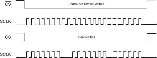 Figure 68. SCLK Clocking Methods
9.5.1.3 Data Input Pin (DIN)
The data input pin (DIN) is used along with SCLK to communicate with the ADS129x (opcode commands and register data). The device latches data on DIN on the falling edge of SCLK.
9.5.1.4 Data Output Pin (DOUT)
The data output pin (DOUT) is used with SCLK to read conversion and register data from the ADS129x. Data on DOUT are shifted out on the rising edge of SCLK. DOUT goes to a high-impedance state when CS is high. In read data continuous mode (see the SPI Command Definitions section for more details), the DOUT output line also indicates when new data are available. Use this feature to minimize the number of connections between the device and the system controller.
Figure 69 shows the data output protocol for ADS1298.
 Figure 69. SPI Bus Data Output for the ADS1298 (Eight Channels)
9.5.2 SPI Command Definitions
The ADS129x provide flexible configuration control. The opcode commands, summarized in Table 15, control and configure the operation of the ADS129x. The opcode commands are stand-alone, except for the register read and register write operations that require a second command byte plus data. CS can be taken high or held low between opcode commands, but must stay low for the entire command operation (especially for multibyte commands). System opcode commands and the RDATA command are decoded by the ADS129x on the seventh falling edge of SCLK. The register read and write opcodes are decoded on the eighth SCLK falling edge. Be sure to follow SPI timing requirements when pulling CS high after issuing a command.
Table 15. Opcode Command Definitions
| COMMAND | DESCRIPTION | FIRST BYTE | SECOND BYTE |
|---|---|---|---|
| SYSTEM COMMANDS | |||
| WAKEUP | Wakeup from standby mode | 0000 0010 (02h) | — |
| STANDBY | Enter standby mode | 0000 0100 (04h) | — |
| RESET | Reset the device | 0000 0110 (06h) | — |
| START | Start/restart (synchronize) conversions | 0000 1000 (08h) | — |
| STOP | Stop conversion | 0000 1010 (0Ah) | — |
| DATA READ COMMANDS | |||
| RDATAC | Enable Read Data Continuous mode. This mode is the default mode at power up.(2) |
0001 0000 (10h) | — |
| SDATAC | Stop Read Data Continuously mode | 0001 0001 (11h) | — |
| RDATA | Read data by command; supports multiple read back. | 0001 0010 (12h) | — |
| REGISTER READ COMMANDS | |||
| RREG | Read n nnnn registers starting at address r rrrr | 001r rrrr (2xh)(1) | 000n nnnn(1) |
| WREG | Write n nnnn registers starting at address r rrrr | 010r rrrr (4xh)(1) | 000n nnnn(1) |
9.5.2.1 WAKEUP: Exit Standby Mode
The WAKEUP opcode exits low-power standby mode; see the STANDBY: Enter Standby Mode section. Time is required when exiting standby mode (see the Electrical Characteristics for details). There are no restrictions on the SCLK rate for this command; issue this command at any time. Any subsequent command must be sent after 4 tCLK cycles.
9.5.2.2 STANDBY: Enter Standby Mode
The STANDBY opcode command enters low-power standby mode. All parts of the circuit are shut down except for the reference section. Standby mode power consumption is specified in the Electrical Characteristics. There are no restrictions on the SCLK rate for this command; issue this command at any time. Send a WAKEUP command to return device to normal operation. Serial interface is active; therefore, register read and write commands are permitted while in this mode.
9.5.2.3 RESET: Reset Registers to Default Values
The RESET command resets the digital filter cycle and returns all register settings to the respective default values. See the Reset (RESET Pin and Reset Command) section for more details. There are no restrictions on the SCLK rate for this command; issue this command at any time. 18 tCLK cycles are required to execute the RESET command. Do not send any commands during this time.
9.5.2.4 START: Start Conversions
This opcode starts data conversions. Tie the START pin low to control conversions by command. If conversions are in progress this command has no effect. The STOP opcode command is used to stop conversions. If the START command is immediately followed by a STOP command, there must be a gap of 4 tCLK cycles between the two commands. When the START opcode is sent to the device, keep the START pin low until the STOP command is issued. (See the Start Mode subsection of the SPI Interface section for more details.) There are no restrictions on the SCLK rate for this command and it can be issued any time.
9.5.2.5 STOP: Stop Conversions
The STOP opcode stops conversions. Tie the START pin low to control conversions by command. When the STOP command is sent, the conversion in progress completes and further conversions are stopped. If conversions are already stopped, this command has no effect. There are no restrictions on the SCLK rate for this command; issue this command at any time.
9.5.2.6 RDATAC: Read Data Continuous
The RDATAC opcode enables the output of conversion data on each DRDY without the need to issue subsequent read data opcodes. This opcode places the conversion data in the output register where it may be shifted out directly. The read data continuous mode is the default mode of the device and the device defaults to this mode on power up and reset.
RDATAC mode is cancelled by the stop read data continuous command (SDATAC). If the device is in RDATAC mode, an SDATAC command must be issued before any other commands can be sent to the device. There is no restriction on the SCLK rate for this command. However, subsequent data retrieval SCLKs or the SDATAC opcode command must wait at least 4 tCLK cycles. As shown in Figure 70, the timing for RDATAC illustrates the keep-out zone of 4 tCLK periods around the DRDY pulse when this command cannot be issued. If no data are retrieved from the device, DOUT and DRDY behave similarly in this mode. To retrieve data from the device after RDATAC command is issued, make sure that either the START pin is high or the START command is issued. Figure 70 shows the recommended way to use the RDATAC command. RDATAC is ideally suited for applications such as data loggers or recorders, where registers are set once and do not need to be reconfigured.

9.5.2.7 SDATAC: Stop Read Data Continuous
This SDATAC opcode command cancels read data continuous (RDATAC) mode. There is no restriction on the SCLK rate for this command, but the next command must wait for 4 tCLK cycles.
9.5.2.8 RDATA: Read Data
Issue the RDATA command after DRDY goes low to read the conversion result (in SDATAC mode). There is no restriction on the SCLK rate for this command, and there is no wait time needed for the subsequent commands or data retrieval SCLKs. To retrieve data from the device after RDATA command is issued, make sure that either the START pin is high or the START command is issued. When reading data with the RDATA command, the read operation can overlap the occurrence of the next DRDY without data corruption. Figure 71 shows the recommended way to use the RDATA command. RDATA is best suited for ECG- and EEG-type systems, where register settings must be read or changed often between conversion cycles.
 Figure 71. RDATA Usage
9.5.2.9 Sending Multibyte Commands
The ADS129x serial interface decodes commands in bytes, and requires 4 tCLK periods to decode and execute. Therefore, when sending multibyte commands, a 4 tCLK period must separate the end of one byte (or opcode) and the next.
For example, if CLK is 2.048 MHz, then tSDECODE (4 × tCLK) is 1.96 µs. When SCLK is 16 MHz, the maximum transfer speed for one byte is 500 ns. This byte transfer time does not meet the tSDECODE specification; therefore, a delay must be inserted so that the end of the second byte arrives 1.46 µs later. However, if SCLK is 4 MHz, one byte is transferred in 2 µs. Because this transfer time exceeds the tSDECODE specification, the processor can send subsequent bytes without delay. In the second scenario, the serial port can be programmed to use multiple-byte transfers instead of the single-byte transfers required to meet the timing of the first scenario .
9.5.2.10 RREG: Read From Register
The RREG opcode command reads register data. The RREG command is a two-byte opcode followed by the output of the register data. The first byte contains the command opcode and the register address. The second byte of the opcode specifies the number of registers to read – 1.
First opcode byte: 001r rrrr, where r rrrr is the starting register address.
Second opcode byte: 000n nnnn, where n nnnn is the number of registers to read – 1.
The 17th SCLK rising edge of the operation clocks out the MSB of the first register, as shown in Figure 72. When the device is in read data continuous mode, it is necessary to issue a SDATAC command before a RREG command can be issued. An RREG command can be issued any time. However, because this command is a multibyte command, there are restrictions on the SCLK rate depending on the way the SCLKs are issued. See the Serial Clock (SCLK)section for more details. CS must be low for the entire command.
 Figure 72. RREG Command Example: Read Two Registers Starting from Register 00h (ID Register)
(OPCODE 1 = 0010 0000, OPCODE 2 = 0000 0001)
9.5.2.11 WREG: Write to Register
The WREG opcode command writes register data. The WREG command is a two-byte opcode followed by the input of the register data. The first byte contains the command opcode and the register address. The second byte of the opcode specifies the number of registers to write – 1.
First opcode byte: 010r rrrr, where r rrrr is the starting register address.
Second opcode byte: 000n nnnn, where n nnnn is the number of registers to write – 1.
After the opcode bytes, the register data follows (in MSB-first format), as shown in Figure 73. The WREG command can be issued any time. However, because this command is a multibyte command, there are restrictions on the SCLK rate depending on the way the SCLKs are issued. See the Serial Clock (SCLK) section for more details. CS must be low for the entire command.
 Figure 73. WREG Command Example: Write Two Registers Starting from 00h (ID Register)
(OPCODE 1 = 0100 0000, OPCODE 2 = 0000 0001)
9.6 Register Maps
Table 16 lists the various ADS129x registers.
Table 16. Register Assignments
| ADDRESS | REGISTER | RESET VALUE (Hex) | BIT 7 | BIT 6 | BIT 5 | BIT 4 | BIT 3 | BIT 2 | BIT 1 | BIT 0 |
|---|---|---|---|---|---|---|---|---|---|---|
| DEVICE SETTINGS (READ-ONLY REGISTERS) | ||||||||||
| 00h | ID | xx | DEV_ID7 | DEV_ID6 | DEV_ID5 | 1 | 0 | DEV_ID2 | DEV_ID1 | DEV_ID0 |
| GLOBAL SETTINGS ACROSS CHANNELS | ||||||||||
| 01h | CONFIG1 | 06 | HR | DAISY_EN | CLK_EN | 0 | 0 | DR2 | DR1 | DR0 |
| 02h | CONFIG2 | 40 | 0 | 0 | WCT_CHOP | INT_TEST | 0 | TEST_AMP | TEST_FREQ1 | TEST_FREQ0 |
| 03h | CONFIG3 | 40 | PD_REFBUF | 1 | VREF_4V | RLD_MEAS | RLDREF_INT | PD_RLD | RLD_LOFF_ SENS |
RLD_STAT |
| 04h | LOFF | 00 | COMP_TH2 | COMP_TH1 | COMP_TH0 | VLEAD_OFF_ EN | ILEAD_OFF1 | ILEAD_OFF0 | FLEAD_OFF1 | FLEAD_OFF0 |
| CHANNEL-SPECIFIC SETTINGS | ||||||||||
| 05h | CH1SET | 00 | PD1 | GAIN12 | GAIN11 | GAIN10 | 0 | MUX12 | MUX11 | MUX10 |
| 06h | CH2SET | 00 | PD2 | GAIN22 | GAIN21 | GAIN20 | 0 | MUX22 | MUX21 | MUX20 |
| 07h | CH3SET | 00 | PD3 | GAIN32 | GAIN31 | GAIN30 | 0 | MUX32 | MUX31 | MUX30 |
| 08h | CH4SET | 00 | PD4 | GAIN42 | GAIN41 | GAIN40 | 0 | MUX42 | MUX41 | MUX40 |
| 09h | CH5SET(1) | 00 | PD5 | GAIN52 | GAIN51 | GAIN50 | 0 | MUX52 | MUX51 | MUX50 |
| 0Ah | CH6SET(1) | 00 | PD6 | GAIN62 | GAIN61 | GAIN60 | 0 | MUX62 | MUX61 | MUX60 |
| 0Bh | CH7SET(1) | 00 | PD7 | GAIN72 | GAIN71 | GAIN70 | 0 | MUX72 | MUX71 | MUX70 |
| 0Ch | CH8SET(1) | 00 | PD8 | GAIN82 | GAIN81 | GAIN80 | 0 | MUX82 | MUX81 | MUX80 |
| 0Dh | RLD_SENSP(2) | 00 | RLD8P(1) | RLD7P(1) | RLD6P(1) | RLD5P(1) | RLD4P | RLD3P | RLD2P | RLD1P |
| 0Eh | RLD_SENSN(2) | 00 | RLD8N(1) | RLD7N(1) | RLD6N(1) | RLD5N(1) | RLD4N | RLD3N | RLD2N | RLD1N |
| 0Fh | LOFF_SENSP(2) | 00 | LOFF8P | LOFF7P | LOFF6P | LOFF5P | LOFF4P | LOFF3P | LOFF2P | LOFF1P |
| 10h | LOFF_SENSN(2) | 00 | LOFF8N | LOFF7N | LOFF6N | LOFF5N | LOFF4N | LOFF3N | LOFF2N | LOFF1N |
| 11h | LOFF_FLIP | 00 | LOFF_FLIP8 | LOFF_FLIP7 | LOFF_FLIP6 | LOFF_FLIP5 | LOFF_FLIP4 | LOFF_FLIP3 | LOFF_FLIP2 | LOFF_FLIP1 |
| LEAD-OFF STATUS REGISTERS (READ-ONLY REGISTERS) | ||||||||||
| 12h | LOFF_STATP | 00 | IN8P_OFF | IN7P_OFF | IN6P_OFF | IN5P_OFF | IN4P_OFF | IN3P_OFF | IN2P_OFF | IN1P_OFF |
| 13h | LOFF_STATN | 00 | IN8N_OFF | IN7N_OFF | IN6N_OFF | IN5N_OFF | IN4N_OFF | IN3N_OFF | IN2N_OFF | IN1N_OFF |
| GPIO AND OTHER REGISTERS | ||||||||||
| 14h | GPIO | 0F | GPIOD4 | GPIOD3 | GPIOD2 | GPIOD1 | GPIOC4 | GPIOC3 | GPIOC2 | GPIOC1 |
| 15h | PACE | 00 | 0 | 0 | 0 | PACEE1 | PACEE0 | PACEO1 | PACEO0 | PD_PACE |
| 16h | RESP | 00 | RESP_ DEMOD_EN1 |
RESP_MOD_EN1 | 1 | RESP_PH2 | RESP_PH1 | RESP_PH0 | RESP_CTRL1 | RESP_CTRL0 |
| 17h | CONFIG4 | 00 | RESP_FREQ2 | RESP_FREQ1 | RESP_FREQ0 | 0 | SINGLE_ SHOT |
WCT_TO_ RLD |
PD_LOFF_
COMP |
0 |
| 18h | WCT1 | 00 | aVF_CH6 | aVL_CH5 | aVR_CH7 | avR_CH4 | PD_WCTA | WCTA2 | WCTA1 | WCTA0 |
| 19h | WCT2 | 00 | PD_WCTC | PD_WCTB | WCTB2 | WCTB1 | WCTB0 | WCTC2 | WCTC1 | WCTC0 |
9.6.1 Register Descriptions
The read-only ID control register is programmed during device manufacture to indicate device characteristics.
9.6.1.1 ID: ID Control Register (address = 00h) (reset = xxh)
| 7 | 6 | 5 | 4 | 3 | 2 | 1 | 0 |
| DEV_ID[7:5] | 1 | 0 | DEV_ID[2:0] | ||||
| R-x | R-2h | R-x | |||||
| LEGEND: R/W = Read/Write; R = Read only; -n = value after reset |
Table 17. ID Control Register Field Descriptions
| Bit | Field | Type | Reset | Description |
|---|---|---|---|---|
| 7:5 | DEV_ID[7:5] | R | xh | Device ID
These bits indicate the device family. 000 = Reserved 011 = Reserved 100 = ADS129x device family 101 = Reserved 110 = ADS129xR device family 111 = Reserved |
| 4:3 | RESERVED | R | 2h | Reserved
Always read back 2h |
| 2:0 | DEV_ID[2:0] | R | xh | Channel ID
These bits indicates number of channels. 000 = 4-channel ADS1294 or ADS1294R 001 = 6-channel ADS1296 or ADS1296R 010 = 8-channel ADS1298 or ADS1298R 011 = Reserved 111 = Reserved |
9.6.1.2 CONFIG1: Configuration Register 1 (address = 01h) (reset = 06h)
| 7 | 6 | 5 | 4 | 3 | 2 | 1 | 0 |
| HR | DAISY_EN | CLK_EN | 0 | 0 | DR[2:0] | ||
| R/W-0h | R/W-0h | R/W-0h | R/W-0h | R/W-6h | |||
| LEGEND: R/W = Read/Write; R = Read only; -n = value after reset |
Table 18. Configuration Register 1 Field Descriptions
| Bit | Field | Type | Reset | Description |
|---|---|---|---|---|
| 7 | HR | R/W | 0h | High-resolution or low-power mode
This bit determines whether the device runs in low-power or high-resolution mode. 0 = LP mode 1 = HR mode |
| 6 | DAISY_EN | R/W | 0h | Daisy-chain or multiple readback mode
This bit determines which mode is enabled. 0 = Daisy-chain mode 1 = Multiple readback mode |
| 5 | CLK_EN | R/W | 0h | CLK connection(1)
This bit determines if the internal oscillator signal is connected to the CLK pin when the CLKSEL pin = 1. 0 = Oscillator clock output disabled 1 = Oscillator clock output enabled |
| 4:3 | RESERVED | R/W | 0h | Reserved
Always write 0h |
| 2:0 | DR[2:0] | R/W | 6h | Output data rate
For High-Resolution mode, fMOD = fCLK / 4. For low power mode, fMOD = fCLK / 8. These bits determine the output data rate of the device. 000: fMOD / 16 (HR Mode: 32 kSPS, LP Mode: 16 kSPS) 001: fMOD / 32 (HR Mode: 16 kSPS, LP Mode: 8 kSPS) 010: fMOD / 64 (HR Mode: 8 kSPS, LP Mode: 4 kSPS) 011: fMOD / 128 (HR Mode: 4 kSPS, LP Mode: 2 kSPS) 100: fMOD / 256 (HR Mode: 2 kSPS, LP Mode: 1 kSPS) 101: fMOD / 512 (HR Mode: 1 kSPS, LP Mode: 500 SPS) 110: fMOD / 1024 (HR Mode: 500 SPS, LP Mode: 250 SPS) 111: Reserved (do not use) |
9.6.1.3 CONFIG2: Configuration Register 2 (address = 02h) (reset = 40h)
Configuration register 2 configures the test signal generation. See the Input Multiplexer section for more details.
| 7 | 6 | 5 | 4 | 3 | 2 | 1 | 0 |
| 0 | 0 | WCT_CHOP | INT_TEST | 0 | TEST_AMP | TEST_FREQ[1:0] | |
| R/W-1h | R/W-0h | R/W-0h | R/W-0h | R/W-0h | R/W-0h | ||
| LEGEND: R/W = Read/Write; R = Read only; -n = value after reset |
Table 19. Configuration Register 2 Field Descriptions
| Bit | Field | Type | Reset | Description |
|---|---|---|---|---|
| 7:6 | RESERVED | R/W | 1h | Reserved
Always write 0h |
| 5 | WCT_CHOP | R/W | 0h | WCT chopping scheme
This bit determines whether the chopping frequency of WCT amplifiers is variable or fixed. 0 = Chopping frequency varies, see Table 7 1 = Chopping frequency constant at fMOD / 16 |
| 4 | INT_TEST | R/W | 0h | TEST source
This bit determines the source for the test signal. 0 = Test signals are driven externally 1 = Test signals are generated internally |
| 3 | RESERVED | R/W | 0h | Reserved
Always write 0h |
| 2 | TEST_AMP | R/W | 0h | Test signal amplitude
These bits determine the calibration signal amplitude. 0 = 1 × –(VREFP – VREFN) / 2400 V 1 = 2 × –(VREFP – VREFN) / 2400 V |
| 1:0 | TEST_FREQ[1:0] | R/W | 0h | Test signal frequency
These bits determine the calibration signal frequency. 00 = Pulsed at fCLK / 221 01 = Pulsed at fCLK / 220 10 = Not used 11 = At dc |
9.6.1.4 CONFIG3: Configuration Register 3 (address = 03h) (reset = 40h)
Configuration register 3 configures multireference and RLD operation.
| 7 | 6 | 5 | 4 | 3 | 2 | 1 | 0 |
| PD_REFBUF | 1 | VREF_4V | RLD_MEAS | RLDREF_INT | PD_RLD | RLD_LOFF_SENS | RLD_STAT |
| R/W-0h | R/W-1h | R/W-0h | R/W-0h | R/W-0h | R/W-0h | R/W-0h | R-0h |
| LEGEND: R/W = Read/Write; R = Read only; -n = value after reset |
Table 20. Configuration Register 3 Field Descriptions
| Bit | Field | Type | Reset | Description |
|---|---|---|---|---|
| 7 | PD_REFBUF | R/W | 0h |
Power-down reference buffer This bit determines the power-down reference buffer state. 0 = Power-down internal reference buffer 1 = Enable internal reference buffer |
| 6 | RESERVED | R/W | 1h | Reserved
Always write 1h |
| 5 | VREF_4V | R/W | 0h | Reference voltage
This bit determines the reference voltage, VREFP. 0 = VREFP is set to 2.4 V 1 = VREFP is set to 4 V (use only with a 5-V analog supply) |
| 4 | RLD_MEAS | R/W | 0h | RLD measurement
This bit enables RLD measurement. The RLD signal may be measured with any channel. 0 = Open 1 = RLD_IN signal is routed to the channel that has the MUX_Setting 010 (VREF) |
| 3 | RLDREF_INT | R/W | 0h | RLDREF signal
This bit determines the RLDREF signal source. 0 = RLDREF signal fed externally 1 = RLDREF signal (AVDD – AVSS) / 2 generated internally |
| 2 | PD_RLD | R/W | 0h | RLD buffer power
This bit determines the RLD buffer power state. 0 = RLD buffer is powered down 1 = RLD buffer is enabled |
| 1 | RLD_LOFF_SENS | R/W | 0h | RLD sense function
This bit enables the RLD sense function. 0 = RLD sense is disabled 1 = RLD sense is enabled |
| 0 | RLD_STAT | R | 0h | RLD lead-off status
This bit determines the RLD status. 0 = RLD is connected 1 = RLD is not connected |
9.6.1.5 LOFF: Lead-Off Control Register (address = 04h) (reset = 00h)
The lead-off control register configures the lead-off detection operation.
| 7 | 6 | 5 | 4 | 3 | 2 | 1 | 0 |
| COMP_TH2[2:0] | VLEAD_OFF_EN | ILEAD_OFF[1:0] | FLEAD_OFF[1:0] | ||||
| R/W-0h | R/W-0h | R/W-0h | R/W-0h | ||||
| LEGEND: R/W = Read/Write; R = Read only; -n = value after reset |
Table 21. Lead-Off Control Register Field Descriptions
| Bit | Field | Type | Reset | Description |
|---|---|---|---|---|
| 7:5 | COMP_TH[2:0] | R/W | 0h |
Lead-off comparator threshold Comparator positive side 000 = 95% 001 = 92.5% 010 = 90% 011 = 87.5% 100 = 85% 101 = 80% 110 = 75% 111 = 70% Comparator negative side 000 = 5% 001 = 7.5% 010 = 10% 011 = 12.5% 100 = 15% 101 = 20% 110 = 25% 111 = 30% |
| 4 | VLEAD_OFF_EN | R/W | 0h | Lead-off detection mode
This bit determines the lead-off detection mode. 0 = Current source mode lead-off 1 = pullup or pulldown resistor mode lead-off |
| 3:2 | ILEAD_OFF[1:0] | R/W | 0h | Lead-off current magnitude
These bits determine the magnitude of current for the current lead-off mode. 00 = 6 nA 01 = 12 nA 10 = 18 nA 11 = 24 nA |
| 1:0 | FLEAD_OFF[1:0] | R/W | 0h | Lead-off frequency
These bits determine the frequency of lead-off detect for each channel. 00 = When any bits of the LOFF_SENSP or LOFF_SENSN registers are turned on, make sure that FLEAD[1:0] are either set to 01 or 11 01 = AC lead-off detection at fDR / 4 10 = Do not use 11 = DC lead-off detection turned on |
9.6.1.6 CHnSET: Individual Channel Settings (n = 1 to 8) (address = 05h to 0Ch) (reset = 00h)
The CH[1:8]SET control register configures the power mode, PGA gain, and multiplexer settings channels. See the Input Multiplexer section for details. CH[2:8]SET are similar to CH1SET, corresponding to the respective channels.
| 7 | 6 | 5 | 4 | 3 | 2 | 1 | 0 |
| PDn | GAINn[2:0] | 0 | MUXn[2:0] | ||||
| R/W-0h | R/W-0h | R/W-0h | R/W-0h | ||||
| LEGEND: R/W = Read/Write; R = Read only; -n = value after reset |
Table 22. Individual Channel Settings (n = 1 to 8) Field Descriptions
| Bit | Field | Type | Reset | Description |
|---|---|---|---|---|
| 7 | PDn | R/W | 0h |
Power-down This bit determines the channel power mode for the corresponding channel. 0 = Normal operation 1 = Channel power-down. When powering down a channel, TI recommends that the channel be set to input short by setting the appropriate MUXn[2:0] = 001 of the CHnSET register. |
| 6:4 | GAINn[2:0] | R/W | 0h | PGA gain
These bits determine the PGA gain setting. 000 = 6 001 = 1 010 = 2 011 = 3 100 = 4 101 = 8 110 = 12 |
| 3 | RESERVED | R/W | 0h | Reserved
Always write 0h |
| 2:0 | MUXn[2:0] | R/W | 0h | Channel input
These bits determine the channel input selection. 000 = Normal electrode input 001 = Input shorted (for offset or noise measurements) 010 = Used in conjunction with RLD_MEAS bit for RLD measurements. See the Right Leg Drive (RLD) DC Bias Circuit subsection of the ECG-Specific Functions section for more details. 011 = MVDD for supply measurement 100 = Temperature sensor 101 = Test signal 110 = RLD_DRP (positive electrode is the driver) 111 = RLD_DRN (negative electrode is the driver) |
9.6.1.7 RLD_SENSP: RLD Positive Signal Derivation Register (address = 0Dh) (reset = 00h)
This register controls the selection of the positive signals from each channel for right leg drive (RLD) derivation. See the Right Leg Drive (RLD) DC Bias Circuit section for details.
Registers bits[5:4] are not available for the ADS1294 or ADS1294R. Bits[7:6] are not available for the ADS1294, ADS1294R, ADS1296, or ADS1296R.
| 7 | 6 | 5 | 4 | 3 | 2 | 1 | 0 |
| RLD8P | RLD7P | RLD6P | RLD5P | RLD4P | RLD3P | RLD2P | RLD1P |
| R/W-0h | R/W-0h | R/W-0h | R/W-0h | R/W-0h | R/W-0h | R/W-0h | R/W-0h |
| LEGEND: R/W = Read/Write; R = Read only; -n = value after reset |
Table 23. RLD Positive Signal Derivation Field Descriptions
| Bit | Field | Type | Reset | Description |
|---|---|---|---|---|
| 7 | RLD8P | R/W | 0h | IN8P to RLD
Route channel 8 positive signal into RLD derivation 0: Disabled 1: Enabled |
| 6 | RLD7P | R/W | 0h | IN7P to RLD
Route channel 7 positive signal into RLD derivation 0: Disabled 1: Enabled |
| 5 | RLD6P | R/W | 0h | IN6P to RLD
Route channel 6 positive signal into RLD derivation 0: Disabled 1: Enabled |
| 4 | RLD5P | R/W | 0h | IN5P to RLD
Route channel 5 positive signal into RLD derivation 0: Disabled 1: Enabled |
| 3 | RLD4P | R/W | 0h | IN4P to RLD
Route channel 4 positive signal into RLD derivation 0: Disabled 1: Enabled |
| 2 | RLD3P | R/W | 0h | IN3P to RLD
Route channel 3 positive signal into RLD derivation 0: Disabled 1: Enabled |
| 1 | RLD2P | R/W | 0h | IN2P to RLD
Route channel 2 positive signal into RLD channel 0: Disabled 1: Enabled |
| 0 | RLD1P | R/W | 0h | IN1P to RLD
Route channel 1 positive signal into RLD channel 0: Disabled 1: Enabled |
9.6.1.8 RLD_SENSN: RLD Negative Signal Derivation Register (address = 0Eh) (reset = 00h)
This register controls the selection of the negative signals from each channel for right leg drive derivation. See the Right Leg Drive (RLD) DC Bias Circuit section for details.
Registers bits[5:4] are not available for the ADS1294 and ADS1294R. Bits[7:6] are not available for the ADS1294, ADS1294R, ADS1296, or ADS1296R.
| 7 | 6 | 5 | 4 | 3 | 2 | 1 | 0 |
| RLD8N | RLD7N | RLD6N | RLD5N | RLD4N | RLD3N | RLD2N | RLD1N |
| R/W-0h | R/W-0h | R/W-0h | R/W-0h | R/W-0h | R/W-0h | R/W-0h | R/W-0h |
| LEGEND: R/W = Read/Write; R = Read only; -n = value after reset |
Table 24. RLD Negative Signal Derivation Field Descriptions
| Bit | Field | Type | Reset | Description |
|---|---|---|---|---|
| 7 | RLD8N | R/W | 0h | IN8N to RLD
Route channel 8 negative signal into RLD derivation 0: Disabled 1: Enabled |
| 6 | RLD7N | R/W | 0h | IN7N to RLD
Route channel 7 negative signal into RLD derivation 0: Disabled 1: Enabled |
| 5 | RLD6N | R/W | 0h | IN6N to RLD
Route channel 6 negative signal into RLD derivation 0: Disabled 1: Enabled |
| 4 | RLD5N | R/W | 0h | IN5N to RLD
Route channel 5 negative signal into RLD derivation 0: Disabled 1: Enabled |
| 3 | RLD4N | R/W | 0h | IN4N to RLD
Route channel 4 negative signal into RLD derivation 0: Disabled 1: Enabled |
| 2 | RLD3N | R/W | 0h | IN3N to RLD
Route channel 3 negative signal into RLD derivation 0: Disabled 1: Enabled |
| 1 | RLD2N | R/W | 0h | IN2N to RLD
Route channel 2 negative signal into RLD derivation 0: Disabled 1: Enabled |
| 0 | RLD1N | R/W | 0h | IN1N to RLD
Route channel 1 negative signal into RLD derivation 0: Disabled 1: Enabled |
9.6.1.9 LOFF_SENSP: Positive Signal Lead-Off Detection Register (address = 0Fh) (reset = 00h)
This register selects the positive side from each channel for lead-off detection. See the Lead-Off Detection section for details. The LOFF_STATP register bits are only valid if the corresponding LOFF_SENSP bits are set to 1.
Registers bits[5:4] are not available for the ADS1294 or ADS1294R. Bits[7:6] are not available for the ADS1294, ADS1294R, ADS1296, or ADS1296R.
| 7 | 6 | 5 | 4 | 3 | 2 | 1 | 0 |
| LOFF8P | LOFF7P | LOFF6P | LOFF5P | LOFF4P | LOFF3P | LOFF2P | LOFF1P |
| R/W-0h | R/W-0h | R/W-0h | R/W-0h | R/W-0h | R/W-0h | R/W-0h | R/W-0h |
| LEGEND: R/W = Read/Write; R = Read only; -n = value after reset |
Table 25. Positive Signal Lead-Off Detection Field Descriptions
| Bit | Field | Type | Reset | Description |
|---|---|---|---|---|
| 7 | LOFF8P | R/W | 0h | IN8P lead off
Enable lead-off detection on IN8P 0: Disabled 1: Enabled |
| 6 | LOFF7P | R/W | 0h | IN7P lead off
Enable lead-off detection on IN7P 0: Disabled 1: Enabled |
| 5 | LOFF6P | R/W | 0h | IN6P lead off
Enable lead-off detection on IN6P 0: Disabled 1: Enabled |
| 4 | LOFF5P | R/W | 0h | IN5P lead off
Enable lead-off detection on IN5P 0: Disabled 1: Enabled |
| 3 | LOFF4P | R/W | 0h | IN4P lead off
Enable lead-off detection on IN4P 0: Disabled 1: Enabled |
| 2 | LOFF3P | R/W | 0h | IN3P lead off
Enable lead-off detection on IN3P 0: Disabled 1: Enabled |
| 1 | LOFF2P | R/W | 0h | IN2P lead off
Enable lead-off detection on IN2P 0: Disabled 1: Enabled |
| 0 | LOFF1P | R/W | 0h | IN1P lead off
Enable lead-off detection on IN1P 0: Disabled 1: Enabled |
9.6.1.10 LOFF_SENSN: Negative Signal Lead-Off Detection Register (address = 10h) (reset = 00h)
This register selects the negative side from each channel for lead-off detection. See the Lead-Off Detectionsection for details. The LOFF_STATN register bits are only valid if the corresponding LOFF_SENSN bits are set to 1.
Registers bits[5:4] are not available for the ADS1294 or ADS1294R. Bits[7:6] are not available for the ADS1294, ADS1294R, ADS1296, or ADS1296R.
| 7 | 6 | 5 | 4 | 3 | 2 | 1 | 0 |
| LOFF8N | LOFF7N | LOFF6N | LOFF5N | LOFF4N | LOFF3N | LOFF2N | LOFF1N |
| R/W-0h | R/W-0h | R/W-0h | R/W-0h | R/W-0h | R/W-0h | R/W-0h | R/W-0h |
| LEGEND: R/W = Read/Write; R = Read only; -n = value after reset |
Table 26. Negative Signal Lead-Off Detection Field Descriptions
| Bit | Field | Type | Reset | Description |
|---|---|---|---|---|
| 7 | LOFF8N | R/W | 0h | IN8N lead off
Enable lead-off detection on IN8N 0: Disabled 1: Enabled |
| 6 | LOFF7N | R/W | 0h | IN7N lead off
Enable lead-off detection on IN7N 0: Disabled 1: Enabled |
| 5 | LOFF6N | R/W | 0h | IN6N lead off
Enable lead-off detection on IN6N 0: Disabled 1: Enabled |
| 4 | LOFF5N | R/W | 0h | IN5N lead off
Enable lead-off detection on IN5N 0: Disabled 1: Enabled |
| 3 | LOFF4N | R/W | 0h | IN4N lead off
Enable lead-off detectionn on IN4N 0: Disabled 1: Enabled |
| 2 | LOFF3N | R/W | 0h | IN3N lead off
Enable lead-off detectionion on IN3N 0: Disabled 1: Enabled |
| 1 | LOFF2N | R/W | 0h | IN2N lead off
Enable lead-off detectionction on IN2N 0: Disabled 1: Enabled |
| 0 | LOFF1N | R/W | 0h | IN1N lead off
Enable lead-off detectionction on IN1N 0: Disabled 1: Enabled |
9.6.1.11 LOFF_FLIP: Lead-Off Flip Register (address = 11h) (reset = 00h)
This register controls the direction of the current used for lead-off derivation. See the Lead-Off Detectionsection for details.
| 7 | 6 | 5 | 4 | 3 | 2 | 1 | 0 |
| LOFF_FLIP8 | LOFF_FLIP7 | LOFF_FLIP6 | LOFF_FLIP5 | LOFF_FLIP4 | LOFF_FLIP3 | LOFF_FLIP2 | LOFF_FLIP1 |
| R/W-0h | R/W-0h | R/W-0h | R/W-0h | R/W-0h | R/W-0h | R/W-0h | R/W-0h |
| LEGEND: R/W = Read/Write; R = Read only; -n = value after reset |
Table 27. Lead-Off Flip Register Field Descriptions
| Bit | Field | Type | Reset | Description |
|---|---|---|---|---|
| 7 | LOFF_FLIP8 | R/W | 0h | Channel 8 LOFF polarity flip
Flip the pullup/pulldown polarity of the current source or resistor on channel 8 for lead-off derivation. 0: No Flip: IN8P is pulled to AVDD and IN8N pulled to AVSS 1: Flipped: IN8P is pulled to AVSS and IN8N pulled to AVDD |
| 6 | LOFF_FLIP7 | R/W | 0h | Channel 7 LOFF polarity flip
Flip the pullup/pulldown polarity of the current source or resistor on channel 7 for lead-off derivation. 0: No Flip: IN7P is pulled to AVDD and IN7N pulled to AVSS 1: Flipped: IN7P is pulled to AVSS and IN7N pulled to AVDD |
| 5 | LOFF_FLIP6 | R/W | 0h | Channel 6 LOFF polarity flip
Flip the pullup/pulldown polarity of the current source or resistor on channel 6 for lead-off derivation. 0: No Flip: IN6P is pulled to AVDD and IN6N pulled to AVSS 1: Flipped: IN6P is pulled to AVSS and IN6N pulled to AVDD |
| 4 | LOFF_FLIP5 | R/W | 0h | Channel 5 LOFF polarity flip
Flip the pullup/pulldown polarity of the current source or resistor on channel 5 for lead-off derivation. 0: No Flip: IN5P is pulled to AVDD and IN5N pulled to AVSS 1: Flipped: IN5P is pulled to AVSS and IN5N pulled to AVDD |
| 3 | LOFF_FLIP4 | R/W | 0h | Channel 4 LOFF polarity flip
Flip the pullup/pulldown polarity of the current source or resistor on channel 4 for lead-off derivation. 0: No Flip: IN4P is pulled to AVDD and IN4N pulled to AVSS 1: Flipped: IN4P is pulled to AVSS and IN4N pulled to AVDD |
| 2 | LOFF_FLIP3 | R/W | 0h | Channel 3 LOFF polarity flip
Flip the pullup/pulldown polarity of the current source or resistor on channel 3 for lead-off derivation. 0: No Flip: IN3P is pulled to AVDD and IN3N pulled to AVSS 1: Flipped: IN3P is pulled to AVSS and IN3N pulled to AVDD |
| 1 | LOFF_FLIP2 | R/W | 0h | Channel 2 LOFF Polarity Flip
Flip the pullup/pulldown polarity of the current source or resistor on channel 2 for lead-off derivation. 0: No Flip: IN2P is pulled to AVDD and IN2N pulled to AVSS 1: Flipped: IN2P is pulled to AVSS and IN2N pulled to AVDD |
| 0 | LOFF_FLIP1 | R/W | 0h | Channel 1 LOFF Polarity Flip
Flip the pullup/pulldown polarity of the current source or resistor on channel 1 for lead-off derivation. 0: No Flip: IN1P is pulled to AVDD and IN1N pulled to AVSS 1: Flipped: IN1P is pulled to AVSS and IN1N pulled to AVDD |
9.6.1.12 LOFF_STATP: Lead-Off Positive Signal Status Register (address = 12h) (reset = 00h)
This register stores the status of whether the positive electrode on each channel is on or off. See the Lead-Off Detection section for details. Ignore the LOFF_STATP values if the corresponding LOFF_SENSP bits are not set to 1.
When the LOFF_SENSEP bits are 0, the LOFF_STATP bits should be ignored.
| 7 | 6 | 5 | 4 | 3 | 2 | 1 | 0 |
| IN8P_OFF | IN7P_OFF | IN6P_OFF | IN5P_OFF | IN4P_OFF | IN3P_OFF | IN2P_OFF | IN1P_OFF |
| R-0h | R-0h | R-0h | R-0h | R-0h | R-0h | R-0h | R-0h |
| LEGEND: R/W = Read/Write; R = Read only; -n = value after reset |
Table 28. Lead-Off Positive Signal Status Field Descriptions
| Bit | Field | Type | Reset | Description |
|---|---|---|---|---|
| 7 | IN8P_OFF | R | 0h | Channel 8 positive channel lead-off status
Status of whether IN8P electrode is on or off 0: Electrode is on 1: Electrode is off |
| 6 | IN7P_OFF | R | 0h | Channel 7 positive channel lead-off status
Status of whether IN7P electrode is on or off 0: Electrode is on 1: Electrode is off |
| 5 | IN6P_OFF | R | 0h | Channel 6 positive channel lead-off status
Status of whether IN6P electrode is on or off 0: Electrode is on 1: Electrode is off |
| 4 | IN5P_OFF | R | 0h | Channel 5 positive channel lead-off status
Status of whether IN5P electrode is on or off 0: Electrode is on 1: Electrode is off |
| 3 | IN4P_OFF | R | 0h | Channel 4 positive channel lead-off status
Status of whether IN4P electrode is on or off 0: Electrode is on 1: Electrode is off |
| 2 | IN3P_OFF | R | 0h | Channel 3 positive channel lead-off status
Status of whether IN3P electrode is on or off 0: Electrode is on 1: Electrode is off |
| 1 | IN2P_OFF | R | 0h | Channel 2 positive channel lead-off status
Status of whether IN2P electrode is on or off 0: Electrode is on 1: Electrode is off |
| 0 | IN1P_OFF | R | 0h | Channel 1 positive channel lead-off status
Status of whether IN1P electrode is on or off 0: Electrode is on 1: Electrode is off |
9.6.1.13 LOFF_STATN: Lead-Off Negative Signal Status Register (address = 13h) (reset = 00h)
This register stores the status of whether the negative electrode on each channel is on or off. See the Lead-Off Detection section for details. Ignore the LOFF_STATN values if the corresponding LOFF_SENSN bits are not set to 1.
When the LOFF_SENSEN bits are 0, the LOFF_STATP bits should be ignored.
| 7 | 6 | 5 | 4 | 3 | 2 | 1 | 0 |
| IN8N_OFF | IN7N_OFF | IN6N_OFF | IN5N_OFF | IN4N_OFF | IN3N_OFF | IN2N_OFF | IN1N_OFF |
| R-0h | R-0h | R-0h | R-0h | R-0h | R-0h | R-0h | R-0h |
| LEGEND: R/W = Read/Write; R = Read only; -n = value after reset |
Table 29. Lead-Off Negative Signal Status Field Descriptions
| Bit | Field | Type | Reset | Description |
|---|---|---|---|---|
| 7 | IN8N_OFF | R | 0h | Channel 8 negative channel lead-off status
Status of whether IN8N electrode is on or off 0: Electrode is on 1: Electrode is off |
| 6 | IN7N_OFF | R | 0h | Channel 7 negative channel lead-off status
Status of whether IN7N electrode is on or off 0: Electrode is on 1: Electrode is off |
| 5 | IN6N_OFF | R | 0h | Channel 6 negative channel lead-off status
Status of whether IN6N electrode is on or off 0: Electrode is on 1: Electrode is off |
| 4 | IN5N_OFF | R | 0h | Channel 5 negative channel lead-off status
Status of whether IN5N electrode is on or off 0: Electrode is on 1: Electrode is off |
| 3 | IN4N_OFF | R | 0h | Channel 4 negative channel lead-off status
Status of whether IN4N electrode is on or off 0: Electrode is on 1: Electrode is off |
| 2 | IN3N_OFF | R | 0h | Channel 3 negative channel lead-off status
Status of whether IN3N electrode is on or off 0: Electrode is on 1: Electrode is off |
| 1 | IN2N_OFF | R | 0h | Channel 2 negative channel lead-off status
Status of whether IN2N electrode is on or off 0: Electrode is on 1: Electrode is off |
| 0 | IN1N_OFF | R | 0h | Channel 1 negative channel lead-off status
Status of whether IN1N electrode is on or off 0: Electrode is on 1: Electrode is off |
9.6.1.14 GPIO: General-Purpose I/O Register (address = 14h) (reset = 0Fh)
The general-purpose I/O register controls the action of the three GPIO pins. When RESP_CTRL[1:0] is in mode 01 and 11, the GPIO2, GPIO3, and GPIO4 pins are not available for use.
| 7 | 6 | 5 | 4 | 3 | 2 | 1 | 0 |
| GPIOD[4:1] | GPIOC[4:1] | ||||||
| R/W-0h | R/W-Fh | ||||||
| LEGEND: R/W = Read/Write; R = Read only; -n = value after reset |
Table 30. General-Purpose I/O Field Descriptions
| Bit | Field | Type | Reset | Description |
|---|---|---|---|---|
| 7:4 | GPIOD[4:1] | R/W | 0h | GPIO data
These bits are used to read and write data to the GPIO ports. When reading the register, the data returned correspond to the state of the GPIO external pins, whether they are programmed as inputs or as outputs. As outputs, a write to the GPIOD sets the output value. As inputs, a write to the GPIOD has no effect. GPIO is not available in certain respiration modes. |
| 3:0 | GPIOC[4:1] | R/W | Fh | GPIO control (corresponding GPIOD)
These bits determine if the corresponding GPIOD pin is an input or output. 0 = Output 1 = Input |
9.6.1.15 PACE: Pace Detect Register (address = 15h) (reset = 00h)
This register provides the pace controls that configure the channel signal used to feed the external pace detect circuitry. See the Pace Detect section for details.
| 7 | 6 | 5 | 4 | 3 | 2 | 1 | 0 |
| 0 | 0 | 0 | PACEE[1:0] | PACEO[1:0] | PD_PACE | ||
| R/W-0h | R/W-0h | R/W-0h | R/W-0h | R/W-0h | R/W-0h | ||
| LEGEND: R/W = Read/Write; R = Read only; -n = value after reset |
Table 31. (For example, CONTROL_REVISION Register) Field Descriptions
| Bit | Field | Type | Reset | Description |
|---|---|---|---|---|
| 7:5 | RESERVED | R/W | 0h | Reserved
Always write 0h |
| 4:3 | PACEE[1:0] | R/W | 0h | Pace even channels
These bits control the selection of the even number channels available on TEST_PACE_OUT1. Only one channel may be selected at any time. 00 = Channel 2 01 = Channel 4 10 = Channel 6 (ADS1296, ADS1296R, ADS1298, ADS1298R) 11 = Channel 8 (ADS1298 and ADS1298R) |
| 2:1 | PACEO[1:0] | R/W | 0h | Pace odd channels
These bits control the selection of the odd number channels available on TEST_PACE_OUT2. Only one channel may be selected at any time. 00 = Channel 1 01 = Channel 3 10 = Channel 5 (ADS1296, ADS1296R, ADS1298, ADS1298R) 11 = Channel 7 (ADS1298, ADS1298R) |
| 0 | PD_PACE | R/W | 0h | Pace detect buffer
This bit is used to enable/disable the pace detect buffer. 0 = Pace detect buffer turned off 1 = Pace detect buffer turned on |
9.6.1.16 RESP: Respiration Control Register (address = 16h) (reset = 00h)
This register provides the controls for the respiration circuitry; see the Respiration section for details.
| 7 | 6 | 5 | 4 | 3 | 2 | 1 | 0 |
| RESP_ DEMOD_EN1 | RESP_MOD_ EN1 | 1 | RESP_PH[2:0] | RESP_CTRL[1:0] | |||
| R/W-0h | R/W-0h | R/W-0h | R/W-0h | R/W-0h | |||
| LEGEND: R/W = Read/Write; R = Read only; -n = value after reset |
Table 32. Respiration Control Register Field Descriptions
| Bit | Field | Type | Reset | Description |
|---|---|---|---|---|
| 7 | RESP_DEMOD_EN1 | R/W | 0h | Enables respiration demodulation circuitry (ADS129xR only; for ADS129x always write 0)
This bit enables and disables the demodulation circuitry on channel 1. 0 = RESP demodulation circuitry turned off 1 = RESP demodulation circuitry turned on |
| 6 | RESP_MOD_EN1 | R/W | 0h | RESP_MOD_EN1: Enables respiration modulation circuitry (ADS129xR only; for ADS129x always write 0)
This bit enables and disables the modulation circuitry on channel 1. 0 = RESP modulation circuitry turned off 1 = RESP modulation circuitry turned on |
| 5 | RESERVED | R/W | 0h | Reserved
Always write 1h |
| 4:2 | RESP_PH[2:0] | R/W | 0h | Respiration phase(1)
000 = 22.5° 001 = 45° 010 = 67.5° 011 = 90° 100 = 112.5° 101 = 135° 110 = 157.5° 111 = N/A |
| 1:0 | RESP_CTRL[1:0] | R/W | 0h | Respiration control
These bits set the mode of the respiration circuitry. 00 = No respiration 01= External respiration 10 = Internal respiration with internal signals 11 = Internal respiration with user-generated signals |
9.6.1.17 CONFIG4: Configuration Register 4 (address = 17h) (reset = 00h)
| 7 | 6 | 5 | 4 | 3 | 2 | 1 | 0 |
| RESP_FREQ[2:0] | 0 | SINGLE_SHOT | WCT_TO_RLD | PD_LOFF_COMP | 0 | ||
| R/W-0h | R/W-0h | R/W-0h | R/W-0h | R/W-0h | R/W-0h | ||
| LEGEND: R/W = Read/Write; R = Read only; -n = value after reset |
Table 33. Configuration Register 4 Field Descriptions
| Bit | Field | Type | Reset | Description |
|---|---|---|---|---|
| 7:5 | RESP_FREQ[2:0] | R/W | 0h | Respiration modulation frequency
These bits control the respiration control frequency when RESP_CTRL[1:0] = 10 or RESP_CTRL[1:0] = 10(1). 000 = 64 kHz modulation clock 001 = 32 kHz modulation clock 010 = 16kHz square wave on GPIO3 and GPIO04. Output on GPIO4 is 180 degree out of phase with GPIO3. 011 = 8kHz square wave on GPIO3 and GPIO04. Output on GPIO4 is 180 degree out of phase with GPIO3. 100 = 4kHz square wave on GPIO3 and GPIO04. Output on GPIO4 is 180 degree out of phase with GPIO3. 101 = 2kHz square wave on GPIO3 and GPIO04. Output on GPIO4 is 180 degree out of phase with GPIO3. 110 = 1kHz square wave on GPIO3 and GPIO04. Output on GPIO4 is 180 degree out of phase with GPIO3. 111 = 500Hz square wave on GPIO3 and GPIO04. Output on GPIO4 is 180 degree out of phase with GPIO3. Modes 000 and 001 are modulation frequencies in internal and external respiration modes. In internal respiration mode, the control signals appear at the RESP_MODP and RESP_MODN terminals. All other bit settings generate square waves as described above on GPIO4 and GPIO3. |
| 4 | RESERVED | R/W | 0h | Reserved
Always write 0h |
| 3 | SINGLE_SHOT | R/W | 0h | Single-shot conversion
This bit sets the conversion mode. 0 = Continuous conversion mode 1 = Single-shot mode |
| 2 | WCT_TO_RLD | R/W | 0h | Connects the WCT to the RLD
This bit connects WCT to RLD. 0 = WCT to RLD connection off 1 = WCT to RLD connection on |
| 1 | PD_LOFF_COMP | R/W | 0h | Lead-off comparator power-down
This bit powers down the lead-off comparators. 0 = Lead-off comparators disabled 1 = Lead-off comparators enabled |
| 0 | RESERVED | R/W | 0h | Reserved
Always write 0h |
9.6.1.18 WCT1: Wilson Central Terminal and Augmented Lead Control Register (address = 18h) (reset = 00h)
The WCT1 control register configures the device WCT circuit channel selection and the augmented leads.
| 7 | 6 | 5 | 4 | 3 | 2 | 1 | 0 |
| aVF_CH6 | aVL_CH5 | aVR_CH7 | aVR_CH4 | PD_WCTA | WCTA[2:0] | ||
| R/W-0h | R/W-0h | R/W-0h | R/W-0h | R/W-0h | R/W-0h | ||
| LEGEND: R/W = Read/Write; R = Read only; -n = value after reset |
Table 34. Wilson Central Terminal and Augmented Lead Control Field Descriptions
| Bit | Field | Type | Reset | Description |
|---|---|---|---|---|
| 7 | aVF_CH6 | R/W | 0h | Enable (WCTA + WCTB)/2 to the negative input of channel 6 (ADS1296, ADS1296R, ADS1298, and ADS1298R)
0 = Disabled 1 = Enabled |
| 6 | aVL_CH5 | R/W | 0h | Enable (WCTA + WCTC)/2 to the negative input of channel 5 (ADS1296, ADS1296R, ADS1298, and ADS1298R)
0 = Disabled 1 = Enabled |
| 5 | aVR_CH7 | R/W | 0h | Enable (WCTB + WCTC)/2 to the negative input of channel 7 (ADS1298 and ADS1298R)
0 = Disabled 1 = Enabled |
| 4 | aVR_CH4 | R/W | 0h | Enable (WCTB + WCTC)/2 to the negative input of channel 4
0 = Disabled 1 = Enabled |
| 3 | PD_WCTA | R/W | 0h | Power-down WCTA
0 = Powered down 1 = Powered on |
| 2:0 | WCTA[2:0] | R/W | 0h | WCT Amplifier A channel selection, typically connected to RA electrode
These bits select one of the eight electrode inputs of channels 1 to 4. 000 = Channel 1 positive input connected to WCTA amplifier 001 = Channel 1 negative input connected to WCTA amplifier 010 = Channel 2 positive input connected to WCTA amplifier 011 = Channel 2 negative input connected to WCTA amplifier 100 = Channel 3 positive input connected to WCTA amplifier 101 = Channel 3 negative input connected to WCTA amplifier 110 = Channel 4 positive input connected to WCTA amplifier 111 = Channel 4 negative input connected to WCTA amplifier |
9.6.1.19 WCT2: Wilson Central Terminal Control Register (address = 18h) (reset = 00h)
The WCT2 configuration register configures the device WCT circuit channel selection.
| 7 | 6 | 5 | 4 | 3 | 2 | 1 | 0 |
| PD_WCTC | PD_WCTB | WCTB[2:0] | WCTC[2:0] | ||||
| R/W-0h | R/W-0h | R/W-0h | R/W-0h | ||||
| LEGEND: R/W = Read/Write; R = Read only; -n = value after reset |
Table 35. Wilson Central Terminal Control Field Descriptions
| Bit | Field | Type | Reset | Description |
|---|---|---|---|---|
| 7 | PD_WCTC | R/W | 0h | Power-down WCTC
0 = Powered down 1 = Powered on |
| 6 | PD_WCTB | R/W | 0h | Power-down WCTB
0 = Powered down 1 = Powered on |
| 5:3 | WCTB[2:0] | R/W | 0h | WCT amplifier B channel selection, typically connected to LA electrode.
These bits select one of the eight electrode inputs of channels 1 to 4. 000 = Channel 1 positive input connected to WCTB amplifier 001 = Channel 1 negative input connected to WCTB amplifier 010 = Channel 2 positive input connected to WCTB amplifier 011 = Channel 2 negative input connected to WCTB amplifier 100 = Channel 3 positive input connected to WCTB amplifier 101 = Channel 3 negative input connected to WCTB amplifier 110 = Channel 4 positive input connected to WCTB amplifier 111 = Channel 4 negative input connected to WCTB amplifier |
| 2:0 | WCTC[2:0] | R/W | 0h | WCT amplifier C channel selection, typically connected to LL electrode.
These bits select one of the eight electrode inputs of channels 1 to 4. 000 = Channel 1 positive input connected to WCTC amplifier 001 = Channel 1 negative input connected to WCTC amplifier 010 = Channel 2 positive input connected to WCTC amplifier 011 = Channel 2 negative input connected to WCTC amplifier 100 = Channel 3 positive input connected to WCTC amplifier 101 = Channel 3 negative input connected to WCTC amplifier 110 = Channel 4 positive input connected to WCTC amplifier 111 = Channel 4 negative input connected to WCTC amplifier |
