SBAS561C June 2012 – January 2017 ADS131E04 , ADS131E06 , ADS131E08
PRODUCTION DATA.
- 1 Features
- 2 Applications
- 3 Description
- 4 Revision History
- 5 Device Comparison
- 6 Pin Configuration and Functions
- 7 Specifications
- 8 Parameter Measurement Information
-
9 Detailed Description
- 9.1 Overview
- 9.2 Functional Block Diagram
- 9.3 Feature Description
- 9.4 Device Functional Modes
- 9.5
Programming
- 9.5.1 Data Format
- 9.5.2 SPI Interface
- 9.5.3
SPI Command Definitions
- 9.5.3.1 Sending Multibyte Commands
- 9.5.3.2 WAKEUP: Exit STANDBY Mode
- 9.5.3.3 STANDBY: Enter STANDBY Mode
- 9.5.3.4 RESET: Reset Registers to Default Values
- 9.5.3.5 START: Start Conversions
- 9.5.3.6 STOP: Stop Conversions
- 9.5.3.7 OFFSETCAL: Channel Offset Calibration
- 9.5.3.8 RDATAC: Start Read Data Continuous Mode
- 9.5.3.9 SDATAC: Stop Read Data Continuous Mode
- 9.5.3.10 RDATA: Read Data
- 9.5.3.11 RREG: Read from Register
- 9.5.3.12 WREG: Write to Register
- 9.6
Register Map
- 9.6.1
Register Descriptions
- 9.6.1.1 ID: ID Control Register (Factory-Programmed, Read-Only) (address = 00h) [reset = xxh]
- 9.6.1.2 CONFIG1: Configuration Register 1 (address = 01h) [reset = 91h]
- 9.6.1.3 CONFIG2: Configuration Register 2 (address = 02h) [reset = E0h]
- 9.6.1.4 CONFIG3: Configuration Register 3 (address = 03h) [reset = 40]
- 9.6.1.5 FAULT: Fault Detect Control Register (address = 04h) [reset = 00h]
- 9.6.1.6 CHnSET: Individual Channel Settings (address = 05h to 0Ch) [reset = 10h]
- 9.6.1.7 FAULT_STATP: Fault Detect Positive Input Status (address = 12h) [reset = 00h]
- 9.6.1.8 FAULT_STATN: Fault Detect Negative Input Status (address = 13h) [reset = 00h]
- 9.6.1.9 GPIO: General-Purpose IO Register (address = 14h) [reset = 0Fh]
- 9.6.1
Register Descriptions
- 10Application and Implementation
- 11Power Supply Recommendations
- 12Layout
- 13Device and Documentation Support
- 14Mechanical, Packaging, and Orderable Information
パッケージ・オプション
メカニカル・データ(パッケージ|ピン)
- PAG|64
サーマルパッド・メカニカル・データ
- PAG|64
発注情報
11 Power Supply Recommendations
11.1 Power-Up Timing
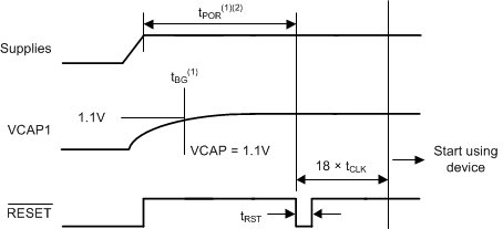
Before device power up, all digital and analog inputs must be low. At the time of power up, keep all of these signals low until the power supplies have stabilized, as shown in Figure 65.
Allow time for the supply voltages to reach their final value, and then begin supplying the master clock signal to the CLK pin. Wait for time tPOR, then transmit a reset pulse using either the RESET pin or RESET command to initialize the digital portion of the chip. Issue the reset after tPOR or after the VCAP1 voltage is greater than 1.1 V, whichever time is longer. Note that:
- tPOR is described in Table 22.
- The VCAP1 pin charge time is set by the RC time constant set by the capacitor value on VCAP1; see Figure 28.
After releasing RESET, the configuration registers must be programmed (see the CONFIG1: Configuration Register 1 (address = 01h) [reset = 91h] subsection of the Register Map section for details) to the desired settings. The power-up sequence timing is shown in Table 22.

Table 22. Timing Requirements for Figure 65
| MIN | MAX | UNIT | ||
|---|---|---|---|---|
| tPOR | Wait after power up until reset | 218 | tCLK | |
| tRST | Reset low duration | 1 | tCLK | |
11.2 Recommended External Capacitor Values
The ADS131E0x power-up time is set by the time required for the critical voltage nodes to settle to their final values. The analog supplies (AVDD and AVSS), digital supply (DVDD), and internal node voltages (VCAPx pins) must be up and stable when the data converter samples are taken to ensure performance. The combined current sourcing capability of the supplies and size of the bypass capacitors dictate the ramp rate of AVDD, AVSS, and DVDD. The VCAPx voltages are charged internally using the supply voltages. Table 23 lists the internal node voltages, their function, and recommended capacitor values to optimize the power-up time.
Table 23. Recommended External Capacitor Values
| PIN | FUNCTION | RECOMMENDED CAPACITOR VALUE | |
|---|---|---|---|
| NAME | NO. | ||
| VCAP1 | 28 | Band-gap voltage for the ADC | 22 µF to AVSS |
| VCAP2 | 30 | Modulator common-mode | 1 µF to AVSS |
| VCAP3 | 55 | PGA charge pump | 0.1 µF || 1 µF to AVSS |
| VCAP4 | 26 | Reference common-mode | 1 µF to AVSS |
| VREFP | 24 | Reference voltage after the internal buffer | 0.1 µF || 10 µF to AVSS |
| AVDD | 19, 21, 22, 56, 59 | Analog supply | 0.1 µF || 1 µF each to AVSS |
| AVDD1 | 54 | Internal PGA charge pump analog supply | 0.1 µF || 1 µF to AVSS1 |
| DVDD | 48, 50 | Digital supply | 0.1 µF || 1 µF each to DGND |
11.3 Device Connections for Unipolar Power Supplies
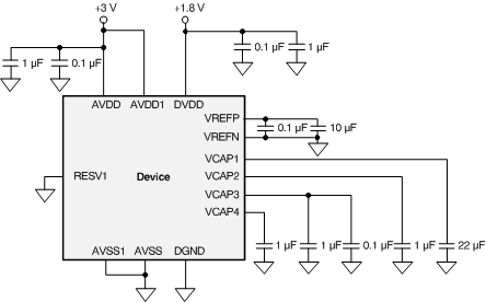
Figure 66 shows the ADS131E0x connected to a unipolar supply. In this example, the analog supply (AVDD) is referenced to the analog ground (AVSS) and the digital supply (DVDD) is referenced to the digital ground (DGND). The ADS131E0x supports an analog supply range of AVDD = 2.7 V to 5.25 V when operated in unipolar supply mode.

NOTE:
Place the supply, reference, and VCAP1 to VCAP4 capacitors as close to the package as possible.11.4 Device Connections for Bipolar Power Supplies
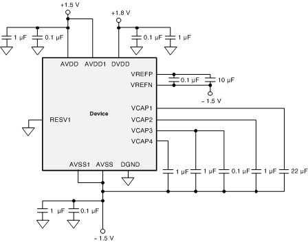
Figure 67 shows the ADS131E0x connected to a bipolar supply. In this example, the analog supply (AVDD) is referenced to the analog ground (AVSS) and the digital supply (DVDD) is referenced to the digital ground (DGND). The ADS131E0x supports an analog supply range of AVDD and AVSS = ±1.5 V to ±2.5 V when operated in bipolar supply mode.

NOTE:
Place the supply, reference, and VCAP1 to VCAP4 capacitors as close to the package as possible.