JAJSNY5 August 2022 ADS131M03-Q1
PRODUCTION DATA
- 1 特長
- 2 アプリケーション
- 3 概要
- 4 Revision History
- 5 Pin Configuration and Functions
- 6 Specifications
- 7 Parameter Measurement Information
-
8 Detailed Description
- 8.1 Overview
- 8.2 Functional Block Diagram
- 8.3
Feature Description
- 8.3.1 Input ESD Protection Circuitry
- 8.3.2 Input Multiplexer
- 8.3.3 Programmable Gain Amplifier (PGA)
- 8.3.4 Voltage Reference
- 8.3.5 Clocking and Power Modes
- 8.3.6 ΔΣ Modulator
- 8.3.7 Digital Filter
- 8.3.8 DC Block Filter
- 8.3.9 Internal Test Signals
- 8.3.10 Channel Phase Calibration
- 8.3.11 Calibration Registers
- 8.3.12 Communication Cyclic Redundancy Check (CRC)
- 8.3.13 Register Map CRC
- 8.4 Device Functional Modes
- 8.5
Programming
- 8.5.1
Interface
- 8.5.1.1 Chip Select (CS)
- 8.5.1.2 Serial Data Clock (SCLK)
- 8.5.1.3 Serial Data Input (DIN)
- 8.5.1.4 Serial Data Output (DOUT)
- 8.5.1.5 Data Ready (DRDY)
- 8.5.1.6 Conversion Synchronization or System Reset (SYNC/RESET)
- 8.5.1.7 SPI Communication Frames
- 8.5.1.8 SPI Communication Words
- 8.5.1.9 ADC Conversion Data
- 8.5.1.10
Commands
- 8.5.1.10.1 NULL (0000 0000 0000 0000)
- 8.5.1.10.2 RESET (0000 0000 0001 0001)
- 8.5.1.10.3 STANDBY (0000 0000 0010 0010)
- 8.5.1.10.4 WAKEUP (0000 0000 0011 0011)
- 8.5.1.10.5 LOCK (0000 0101 0101 0101)
- 8.5.1.10.6 UNLOCK (0000 0110 0101 0101)
- 8.5.1.10.7 RREG (101a aaaa annn nnnn)
- 8.5.1.10.8 WREG (011a aaaa annn nnnn)
- 8.5.1.11 Short SPI Frames
- 8.5.2 Synchronization
- 8.5.1
Interface
- 8.6 ADS131M03-Q1 Registers
- 9 Application and Implementation
- 10Device and Documentation Support
- 11Mechanical, Packaging, and Orderable Information
8.5.1.7 SPI Communication Frames
SPI communication on the ADS131M03-Q1 is performed in frames. Each SPI communication frame consists of several words. The word size is configurable as either 16 bits, 24 bits, or 32 bits by programming the WLENGTH[1:0] bits in the MODE register.
The ADS131M03-Q1 implements a timeout feature for SPI communication. Enable or disable the timeout using the TIMEOUT bit in the MODE register. When enabled, the entire SPI frame (first SCLK to last SCLK) must complete within 215 CLKIN cycles otherwise the SPI resets. This feature is provided as a means to recover SPI synchronization for cases where CS is tied low.
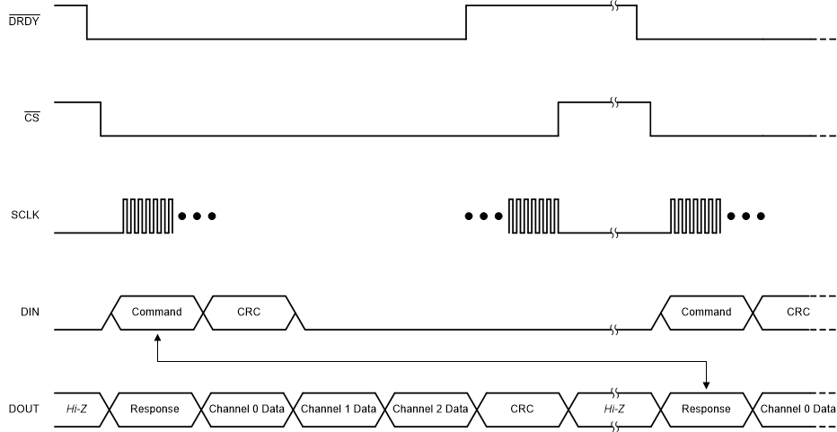
The interface is full duplex, meaning that the interface is capable of transmitting data on DOUT while simultaneously receiving data on DIN. The input frame that the host sends on DIN always begins with a command. The first word on the output frame that the device transmits on DOUT always begins with the response to the command that was written on the previous input frame. The number of words in a command depends on the command provided. For most commands, there are five words in a frame. On DIN, the host provides the command, the command CRC if input CRC is enabled or a word of zeros if input CRC is disabled, and three additional words of zeros. Simultaneously on DOUT, the device outputs the response from the previous frame command, three words of ADC data representing the three ADC channels, and a CRC word. Figure 8-17 illustrates a typical command frame structure.
 Figure 8-17 Typical
Communication Frame
Figure 8-17 Typical
Communication FrameThere are some commands that require more than five words. In the case of a read register (RREG) command where more than a single register is read, the response to the command contains the acknowledgment of the command followed by the register contents requested, which may require a larger frame depending on how many registers are read. See the Section 8.5.1.10.7 section for more details on the RREG command.
In the case of a write register (WREG) command where more than a single register is written, the frame extends to accommodate the additional data. See the Section 8.5.1.10.8 section for more details on the WREG command.
See the Section 8.5.1.10 section for a list of all valid commands and their corresponding responses on the ADS131M03-Q1.
Under special circumstances, a data frame can be shortened by the host. See the Section 8.5.1.11 section for more information about artificially shortening communication frames.