JAJSIN3A February 2020 – February 2021 ADS131M06
PRODUCTION DATA
- 1 特長
- 2 アプリケーション
- 3 概要
- 4 Revision History
- 5 Pin Configuration and Functions
- 6 Specifications
- 7 Parameter Measurement Information
-
8 Detailed Description
- 8.1 Overview
- 8.2 Functional Block Diagram
- 8.3
Feature Description
- 8.3.1 Input ESD Protection Circuitry
- 8.3.2 Input Multiplexer
- 8.3.3 Programmable Gain Amplifier (PGA)
- 8.3.4 Voltage Reference
- 8.3.5 Clocking and Power Modes
- 8.3.6 ΔΣ Modulator
- 8.3.7 Digital Filter
- 8.3.8 DC Block Filter
- 8.3.9 Internal Test Signals
- 8.3.10 Channel Phase Calibration
- 8.3.11 Calibration Registers
- 8.3.12 Communication Cyclic Redundancy Check (CRC)
- 8.3.13 Register Map CRC
- 8.4 Device Functional Modes
- 8.5
Programming
- 8.5.1
Interface
- 8.5.1.1 Chip Select (CS)
- 8.5.1.2 Serial Data Clock (SCLK)
- 8.5.1.3 Serial Data Input (DIN)
- 8.5.1.4 Serial Data Output (DOUT)
- 8.5.1.5 Data Ready (DRDY)
- 8.5.1.6 Conversion Synchronization or System Reset (SYNC/RESET)
- 8.5.1.7 SPI Communication Frames
- 8.5.1.8 SPI Communication Words
- 8.5.1.9 ADC Conversion Data
- 8.5.1.10
Commands
- 8.5.1.10.1 NULL (0000 0000 0000 0000)
- 8.5.1.10.2 RESET (0000 0000 0001 0001)
- 8.5.1.10.3 STANDBY (0000 0000 0010 0010)
- 8.5.1.10.4 WAKEUP (0000 0000 0011 0011)
- 8.5.1.10.5 LOCK (0000 0101 0101 0101)
- 8.5.1.10.6 UNLOCK (0000 0110 0110 0110)
- 8.5.1.10.7 RREG (101a aaaa annn nnnn)
- 8.5.1.10.8 WREG (011a aaaa annn nnnn)
- 8.5.1.11 Short SPI Frames
- 8.5.2 Synchronization
- 8.5.1
Interface
- 8.6 Registers
- 9 Application and Implementation
- 10Power Supply Recommendations
- 11Layout
- 12Device and Documentation Support
- 13Mechanical, Packaging, and Orderable Information
パッケージ・オプション
メカニカル・データ(パッケージ|ピン)
サーマルパッド・メカニカル・データ
発注情報
9.2.3 Application Curves
A source generator was used to provide the voltages and currents to the system. In this design, a nominal voltage of 240 V between the line and neutral, a calibration current of 10 A, and a nominal frequency of 60 Hz were used for each phase.
When the voltages and currents are applied to the system, the design outputs the cumulative active energy pulses and cumulative reactive energy pulses at a rate of 6400 pulses per kilowatt hour. This pulse output was fed into a reference meter that determined the energy percentage error based on the actual energy provided to the system and the measured energy as determined by the active and reactive energy output pulse of the system.
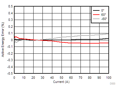
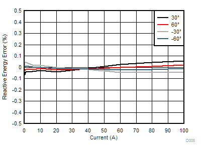
The current was varied from 50 mA to 100 A for the cumulative active energy error and cumulative reactive energy error testing. A phase shift of 0°, 60°, and −60° was applied between the voltage and current waveforms fed to the design for cumulative active energy testing. Based on the error from the active energy output pulse, several plots of active energy percentage error versus current were created for 0°, 60°, and –60° phase shifts. For the cumulative reactive energy error testing, a similar process was followed except that 30°, 60°, –30°, and –60° phase shifts were used, and the cumulative reactive energy error was plotted instead of the cumulative active energy error. In the cumulative active and reactive energy testing, the sum of the energy reading of each phase was tested for accuracy.
In addition to testing active energy by varying current, active energy was also tested by varying the RMS voltage from 240 V to 15 V and measuring the active energy percentage error.
The front-end was calibrated before obtaining the following results. The active energy results are within 0.1% at 0° phase shift. At 60° and –60° phase shift, which is allowed to have relaxed accuracy in electricity meter standards, the trend where the results deviate at higher currents is from the CT phase shift varying across current.
Table 9-3 shows the cumulative active energy accuracy results with changing voltage. Table 9-4 shows the cumulative active energy results with varying current. Figure 9-8 shows a plot of the values in Table 9-4.
| VOLTAGE (V) | % ERROR |
|---|---|
| 240 | 0.0353 |
| 120 | 0.022 |
| 60 | 0.016 |
| 30 | 0.014 |
| 15 | 0.013 |
| CURRENT (A) | 0° | 60° | –60° |
|---|---|---|---|
| 0.05 | 0.019 | 0.045 | –0.032 |
| 0.10 | 0.006 | 0.058 | –0.032 |
| 0.25 | 0.0125 | 0.045 | –0.0385 |
| 0.50 | 0.006 | 0.032 | –0.032 |
| 1.00 | 0.015 | 0.045 | –0.019 |
| 2.00 | 0.003 | 0.045 | –0.039 |
| 5.00 | 0.006 | 0.024 | –0.012 |
| 10.00 | 0.01 | 0.0165 | 0 |
| 20.00 | –0.007 | 0.002 | –0.013 |
| 30.00 | 0.002 | –0.007 | 0.0085 |
| 40.00 | 0 | –0.016 | 0.019 |
| 50.00 | –0.003 | –0.035 | 0.042 |
| 60.00 | 0.002 | –0.047 | 0.053 |
| 70.00 | 0.009 | –0.047 | 0.063 |
| 80.00. | 0.007 | –0.05 | 0.067 |
| 90.00 | 0.013 | –0.045 | 0.08 |
| 100.00 | 0.0223 | –0.04 | 0.092 |
 Figure 9-8 Cumulative Phase Active Energy % Error Versus Current
Table 9-5 shows the cumulative reactive energy accuracy results with changing current. Figure 9-9 shows a plot of the values in Table 9-4.
| CURRENT (A) | 30° | 60° | –30° | –60° |
|---|---|---|---|---|
| 0.05 | –0.003 | 0.004 | –0.023 | –0.027 |
| 0.10 | –0.037 | –0.013 | 0.011 | –0.008 |
| 0.25 | –0.067 | –0.027 | 0.043 | 0.002 |
| 1.00 | –0.044 | –0.021 | 0.0415 | 0.011 |
| 5.00 | –0.036 | –0.0183 | 0.022 | 0.001 |
| 10.00 | –0.03 | –0.012 | 0.014 | –0.003 |
| 20.00 | –0.041 | –0.026 | –0.0035 | –0.013 |
| 40.00 | –0.01 | –0.016 | –0.021 | –0.016 |
| 60.00 | 0.025 | –0.0007 | –0.047 | –0.0247 |
| 80.00 | 0.041 | 0.0085 | –0.048 | –0.021 |
| 100.00 | 0.054 | 0.02 | –0.044 | –0.012 |
 Figure 9-9 Cumulative Reactive Energy % Error Versus Current