SLAS904F October   2012  – May 2016 ADS42LB49 , ADS42LB69

PRODUCTION DATA.  

  1. Features
  2. Applications
  3. Description
  4. Revision History
  5. Pin Configuration and Functions
  6. Specifications
    1. 6.1  Absolute Maximum Ratings
    2. 6.2  ESD Ratings
    3. 6.3  Recommended Operating Conditions
    4. 6.4  Thermal Information
    5. 6.5  Electrical Characteristics: ADS42LB69 (16-Bit)
    6. 6.6  Electrical Characteristics: ADS42LB49 (14-Bit)
    7. 6.7  Electrical Characteristics: General
    8. 6.8  Digital Characteristics
    9. 6.9  Timing Requirements: General
    10. 6.10 Timing Requirements: DDR LVDS Mode
    11. 6.11 Timing Requirements: QDR LVDS Mode
    12. 6.12 Typical Characteristics: ADS42LB69
    13. 6.13 Typical Characteristics: ADS42LB49
    14. 6.14 Typical Characteristics: Common
    15. 6.15 Typical Characteristics: Contour
      1. 6.15.1 Spurious-Free Dynamic Range (SFDR): General
      2. 6.15.2 Signal-to-Noise Ratio (SNR): ADS42LB69
      3. 6.15.3 Signal-to-Noise Ratio (SNR): ADS42LB49
  7. Parameter Measurement Information
  8. Detailed Description
    1. 8.1 Overview
    2. 8.2 Functional Block Diagrams
    3. 8.3 Feature Description
      1. 8.3.1 Digital Gain
      2. 8.3.2 Input Clock Divider
      3. 8.3.3 Overrange Indication
        1. 8.3.3.1 OVR in a QDR Pinout
        2. 8.3.3.2 OVR in a DDR Pinout
        3. 8.3.3.3 Programming Threshold for Fast OVR
      4. 8.3.4 LVDS Buffer
      5. 8.3.5 Output Data Format
    4. 8.4 Device Functional Modes
      1. 8.4.1 Digital Output Information
        1. 8.4.1.1 Output Interface
        2. 8.4.1.2 DDR LVDS Outputs
        3. 8.4.1.3 QDR LVDS Outputs
    5. 8.5 Programming
      1. 8.5.1 Device Configuration
      2. 8.5.2 Details of Serial Interface
        1. 8.5.2.1 Register Initialization
        2. 8.5.2.2 Serial Register Write
        3. 8.5.2.3 Serial Register Readout
    6. 8.6 Register Maps
      1. 8.6.1 Description of Serial Interface Registers
        1. 8.6.1.1  Register 6 (offset = 06h) [reset = 80h]
        2. 8.6.1.2  Register 7 (offset = 07h) [reset = 00h]
        3. 8.6.1.3  Register 8 (offset = 08h) [reset = 00h]
        4. 8.6.1.4  Register B (offset = 0Bh) [reset = 00h]
        5. 8.6.1.5  Register C (offset = 0Ch) [reset = 00h]
        6. 8.6.1.6  Register D (offset = 0Dh) [reset = 6Ch]
        7. 8.6.1.7  Register F (offset = 0Fh) [reset = 00h]
        8. 8.6.1.8  Register 10 (offset = 10h) [reset = 00h]
        9. 8.6.1.9  Register 11 (offset = 11h) [reset = 00h]
        10. 8.6.1.10 Register 12 (offset = 12h) [reset = 00h]
        11. 8.6.1.11 Register 13 (offset = 13h) [reset = 00h]
        12. 8.6.1.12 Register 14 (offset = 14h) [reset = 00h]
        13. 8.6.1.13 Register 15 (offset = 15h) [reset = 00h]
        14. 8.6.1.14 Register 16 (offset = 16h) [reset = 00h]
        15. 8.6.1.15 Register 17 (offset = 17h) [reset = 00h]
        16. 8.6.1.16 Register 18 (offset = 18h) [reset = 00h]
        17. 8.6.1.17 Register 1F (offset = 1Fh) [reset = 7Fh]
        18. 8.6.1.18 Register 20 (offset = 20h) [reset = 00h]
  9. Application and Implementation
    1. 9.1 Application Information
    2. 9.2 Typical Application
      1. 9.2.1 Design Requirements
      2. 9.2.2 Detailed Design Procedure
        1. 9.2.2.1 Analog Input
          1. 9.2.2.1.1 Drive Circuit Requirements
          2. 9.2.2.1.2 Driving Circuit
          3. 9.2.2.1.3 Using the ADS42LBx9 In Time-Domain, Low-Frequency Pulse Applications
        2. 9.2.2.2 Clock Input
        3. 9.2.2.3 SNR and Clock Jitter
      3. 9.2.3 Application Curves
  10. 10Power Supply Recommendations
  11. 11Layout
    1. 11.1 Layout Guidelines
    2. 11.2 Layout Example
  12. 12Device and Documentation Support
    1. 12.1 Related Links
    2. 12.2 Community Resources
    3. 12.3 Trademarks
    4. 12.4 Electrostatic Discharge Caution
    5. 12.5 Glossary
  13. 13Mechanical, Packaging, and Orderable Information

パッケージ・オプション

メカニカル・データ(パッケージ|ピン)
サーマルパッド・メカニカル・データ
発注情報

5 Pin Configuration and Functions

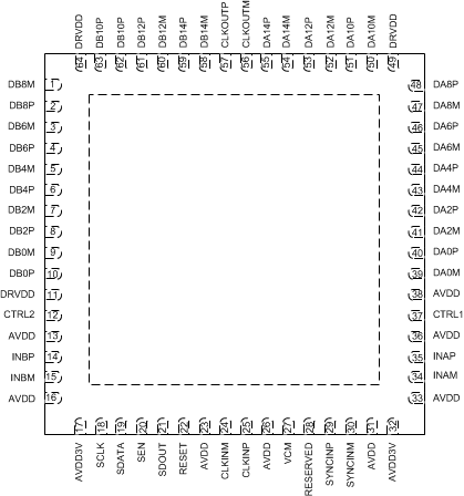
ADS42LB69 DDR LVDS: RGC Package
64-Pin VQFN
Top View
ADS42LB49 ADS42LB69 po_42lb69_las904.gif
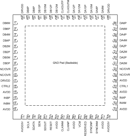
ADS42LB49 DDR LVDS: RGC Package
64-Pin VQFN
Top View
ADS42LB49 ADS42LB69 po_42lb49_las904.gif
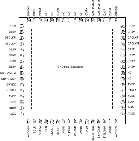
ADS42LB69, ADS42LB49 QDR LVDS: RGC Package
64-Pin VQFN
Top View
ADS42LB49 ADS42LB69 po_2x_ddr_las904.gif

Pin Functions

PIN I/O DESCRIPTION
NAME ADS42LB69
DDR LVDS
ADS42LB49
DDR LVDS
QDR LVDS
INPUT AND REFERENCE
INAP, INAM 35, 34 35, 34 34, 35 I Differential analog input for channel A
INBP, INBM 14, 15 14, 15 14, 15 I Differential analog input for channel B
VCM 27 27 27 O Common-mode voltage for analog inputs, 1.9 V
CLOCK AND SYNC
CLKINP, CLKINM 25, 24 25, 24 24, 25 I Differential clock input for ADC
SYNCINP, SYNCINM 29, 30 29, 30 29, 30 I External sync input. If not used, connect SYNCINP to GND and SYNCINM to AVDD.
CONTROL AND SERIAL
CTRL1 37 37 37 I/O Can be configured as power-down input pin or as OVR output pin for channel A, depending on the register bit PDN/OVR FOR CTRL PINS.
CTRL2 12 12 12 I/O Can be configured as power-down input pin or as OVR output pin for channel B, depending on the register bit PDN/OVR FOR CTRL PINS
NC 39, 40, 55-58, 60, 61 Do not connect
NC/OVR 9, 10, 39, 40 If the OVR ON LSB bit is set, these pins can be used because they carry overrange information. Otherwise, do not connect these pins.
Reserved 28 28 28 Do not connect
RESET 22 22 22 I Hardware reset. Active high.
SCLK 18 18 18 I Serial interface clock input
SDATA 19 19 19 I Serial interface data input
SDOUT 21 21 21 O Serial interface data output
SEN 20 20 20 I Serial interface enable
DATA INTERFACE
CLKOUTP, CLKOUTM 57, 56 57, 56 O Differential LVDS output clock
DA[3:0]P, DA[3:0]M 41-44, 47, 48, 50, 51 O 4-bit QDR LVDS output interface for channel A
DA[14:0]P, DA[14:0]M 39-48, 50-55 41-48, 50-55 O DDR LVDS output interface for channel A
DACLKP, DACLKM 45, 46 O Differential output clock for channel A
DAFRAMEP, DAFRAMEM 52, 53 Differential frame clock output for channel A
DB[3:0]P, DB[3:0]M 1, 2, 5-8, 62, 63 4-bit QDR LVDS output interface for channel B
DB[14:0]P, DB[14:0]M 1-10, 58-63 1-8, 58-63 O DDR LVDS output interface for channel B
DBCLKP, DBCLKM 3, 4 Differential output clock for channel A
DBFRAMEP, DBFRAMEM 9, 10 Differential frame clock output for channel A
OVRA 54 O Overrange indication channel A
OVRB 59 O Overrange indication channel A
POWER SUPPLY
AVDD 13, 16, 23, 26, 31, 33, 36, 38 13, 16, 23, 26, 31, 33, 36, 38 13, 16, 23, 26, 31, 33, 36, 38 I Analog 1.8-V power supply
AVDD3V 17, 32 17, 32 17, 32 I Analog 3.3 V power supply for analog buffer
DRVDD 11, 49, 64 11, 49, 64 11, 49, 64 I Digital 1.8-V power supply
GND Ground pad Ground pad Ground pad I Ground