SLAS525D July 2007 – December 2017 ADS5474
PRODUCTION DATA.
- 1 Features
- 2 Applications
- 3 Description
- 4 Revision History
- 5 Pin Configuration and Functions
- 6 Specifications
- 7 Detailed Description
- 8 Application and Implementation
- 9 Power Supply Recommendations
- 10Layout
- 11Device and Documentation Support
- 12Mechanical, Packaging, and Orderable Information
パッケージ・オプション
メカニカル・データ(パッケージ|ピン)
- PFP|80
サーマルパッド・メカニカル・データ
- PFP|80
発注情報
10 Layout
10.1 Layout Guidelines
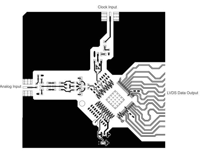
The evaluation board represents a good model of how to lay out the printed circuit board (PCB) to obtain the maximum performance from the ADS5474 device. Follow general design rules such as the use of multilayer boards, a single ground plane for ADC ground connections, and local decoupling ceramic chip capacitors. The analog input traces should be isolated from any external source of interference or noise, including the digital outputs as well as the clock traces. The clock signal traces should also be isolated from other signals, especially in applications such as high IF sampling where low jitter is required. Besides performance-oriented rules, care must be taken when considering the heat dissipation of the device. The thermal heatsink included on the bottom of the package should be soldered to the board as described in the PowerPad Package section. See the ADS5474 EVM User Guide (SLAU194) on the TI web site for the evaluation board schematic.
10.1.1 PowerPAD Package
The PowerPAD package is a thermally-enhanced, standard-size IC package designed to eliminate the use of bulky heatsinks and slugs traditionally used in thermal packages. This package can be easily mounted using standard PCB assembly techniques, and can be removed and replaced using standard repair procedures.
The PowerPAD package is designed so that the leadframe die pad (or thermal pad) is exposed on the bottom of the IC. This pad design provides an extremely low thermal resistance path between the die and the exterior of the package. The thermal pad on the bottom of the IC can then be soldered directly to the PCB, using the PCB as a heatsink.
10.1.1.1 Assembly Process
- Prepare the PCB top-side etch pattern including etch for the leads as well as the thermal pad as illustrated in the Mechanical Data section (at the end of this data sheet).
- Place a 6 × 6 array of thermal vias in the thermal pad area. These holes should be 13 mils (0.013 in or 0.3302 mm) in diameter. The small size prevents wicking of the solder through the holes.
- It is recommended to place a small number of 25-mil (0.025-in or 0.635-mm) diameter holes under the package, but outside the thermal pad area, to provide an additional heat path.
- Connect all holes (both those inside and outside the thermal pad area) to an internal copper plane (such as a ground plane).
- Do not use the typical web or spoke via-connection pattern when connecting the thermal vias to the ground plane. The spoke pattern increases the thermal resistance to the ground plane.
- The top-side solder mask should leave exposed the terminals of the package and the thermal pad area.
- Cover the entire bottom side of the PowerPAD vias to prevent solder wicking.
- Apply solder paste to the exposed thermal pad area and all of the package terminals.
For more detailed information regarding the PowerPAD package and its thermal properties, see either the PowerPAD Made Easy application brief (SLMA004) or the PowerPAD Thermally Enhanced Package application report (SLMA002), both available for download at www.ti.com.
10.2 Layout Example

10.3 Thermal Considerations
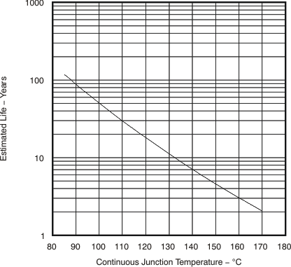
It is important for applications that anticipate running continuously for long periods of time near the maximum-rated ambient temperature of 85°C to consider the data shown in Figure 48. Referring to the Thermal Information table, the worst-case operating condition with no airflow has a thermal rise of 23.7°C/W. At approximately 2.5 W of normal power dissipation, at a maximum ambient of 85°C with no airflow, the junction temperature of the ADS5474 device reaches approximately 85°C + (23.7°C/W × 2.5 W) = +144°C. Being even more conservative and accounting for the maximum possible power dissipation that is ensured (2.797 W), the junction temperature becomes nearly 150°C. As Figure 48 shows, this performance limits the expected lifetime of the ADS5474 device. Operation at 85°C continuously can require airflow or an additional heatsink in order to decrease the internal junction temperature and increase the expected lifetime (because of electromigration failures). An airflow of 250 LFM (linear feet per minute) reduces the thermal resistance to 16.4°C/W and, therefore, the maximum junction temperature to 131°C, assuming a worst-case of 2.797 W and 85°C ambient.
The ADS5474 device performance over temperature is quite good and can be seen starting in Figure 21. Though the typical plots show good performance at 100°C, the device is only rated from –40°C to 85°C. For continuous operation at temperatures near or above the maximum, the expected primary negative effect is a shorter device lifetime because of the electromigration failures at high junction temperatures. The maximum recommended continuous junction temperature is 150°C.
 Figure 48. Operating Life Derating Chart, Electromigration Fail Mode