JAJSH87D April   2015  – April 2019 ADS54J60

PRODUCTION DATA.  

  1. 特長
  2. アプリケーション
  3. 概要
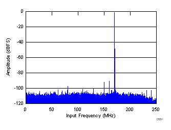
    1.     170MHz の入力信号に対する FFT
  4. 改訂履歴
  5. Device Comparison Table
  6. Pin Configuration and Functions
    1.     Pin Functions
  7. Specifications
    1. 7.1  Absolute Maximum Ratings
    2. 7.2  ESD Ratings
    3. 7.3  Recommended Operating Conditions
    4. 7.4  Thermal Information
    5. 7.5  Electrical Characteristics
    6. 7.6  AC Characteristics
    7. 7.7  Digital Characteristics
    8. 7.8  Timing Requirements
    9. 7.9  Typical Characteristics
    10. 7.10 Typical Characteristics: Contour
  8. Detailed Description
    1. 8.1 Overview
    2. 8.2 Functional Block Diagram
    3. 8.3 Feature Description
      1. 8.3.1 Analog Inputs
      2. 8.3.2 DDC Block
        1. 8.3.2.1 Decimate-by-2 Filter
        2. 8.3.2.2 Decimate-by-4 Filter Using a Digital Mixer
        3. 8.3.2.3 Decimate-by-4 Filter with IQ Outputs
      3. 8.3.3 SYSREF Signal
        1. 8.3.3.1 SYSREF Not Present (Subclass 0, 2)
      4. 8.3.4 Overrange Indication
        1. 8.3.4.1 Fast OVR
      5. 8.3.5 Power-Down Mode
    4. 8.4 Device Functional Modes
      1. 8.4.1 Device Configuration
        1. 8.4.1.1 Serial Interface
        2. 8.4.1.2 Serial Register Write: Analog Bank
        3. 8.4.1.3 Serial Register Readout: Analog Bank
        4. 8.4.1.4 JESD Bank SPI Page Selection
        5. 8.4.1.5 Serial Register Write: JESD Bank
          1. 8.4.1.5.1 Individual Channel Programming
        6. 8.4.1.6 Serial Register Readout: JESD Bank
      2. 8.4.2 JESD204B Interface
        1. 8.4.2.1 JESD204B Initial Lane Alignment (ILA)
        2. 8.4.2.2 JESD204B Test Patterns
        3. 8.4.2.3 JESD204B Frame
        4. 8.4.2.4 JESD204B Frame
        5. 8.4.2.5 JESD204B Frame Assembly with Decimation
          1. 8.4.2.5.1 JESD Transmitter Interface
          2. 8.4.2.5.2 Eye Diagram
    5. 8.5 Register Maps
      1. 8.5.1 Example Register Writes
      2. 8.5.2 Register Descriptions
        1. 8.5.2.1 General Registers
          1. 8.5.2.1.1 Register 0h (address = 0h)
            1. Table 20. Register 0h Field Descriptions
          2. 8.5.2.1.2 Register 1h (address = 1h)
            1. Table 21. Register 1h Field Descriptions
          3. 8.5.2.1.3 Register 2h (address = 2h)
            1. Table 22. Register 2h Field Descriptions
          4. 8.5.2.1.4 Register 3h (address = 3h)
            1. Table 23. Register 3h Field Descriptions
          5. 8.5.2.1.5 Register 4h (address = 4h)
            1. Table 24. Register 4h Field Descriptions
          6. 8.5.2.1.6 Register 5h (address = 5h)
            1. Table 25. Register 5h Field Descriptions
          7. 8.5.2.1.7 Register 11h (address = 11h)
            1. Table 26. Register 11h Field Descriptions
        2. 8.5.2.2 Master Page (080h) Registers
          1. 8.5.2.2.1  Register 20h (address = 20h), Master Page (080h)
            1. Table 27. Registers 20h Field Descriptions
          2. 8.5.2.2.2  Register 21h (address = 21h), Master Page (080h)
            1. Table 28. Register 21h Field Descriptions
          3. 8.5.2.2.3  Register 23h (address = 23h), Master Page (080h)
            1. Table 29. Register 23h Field Descriptions
          4. 8.5.2.2.4  Register 24h (address = 24h), Master Page (080h)
            1. Table 30. Register 24h Field Descriptions
          5. 8.5.2.2.5  Register 26h (address = 26h), Master Page (080h)
            1. Table 31. Register 26h Field Descriptions
          6. 8.5.2.2.6  Register 4Fh (address = 4Fh), Master Page (080h)
            1. Table 32. Register 4Fh Field Descriptions
          7. 8.5.2.2.7  Register 53h (address = 53h), Master Page (080h)
            1. Table 33. Register 53h Field Descriptions
          8. 8.5.2.2.8  Register 54h (address = 54h), Master Page (080h)
            1. Table 34. Register 54h Field Descriptions
          9. 8.5.2.2.9  Register 55h (address = 55h), Master Page (080h)
            1. Table 35. Register 55h Field Descriptions
          10. 8.5.2.2.10 Register 59h (address = 59h), Master Page (080h)
            1. Table 36. Register 59h Field Descriptions
        3. 8.5.2.3 ADC Page (0Fh) Register
          1. 8.5.2.3.1 Register 5F (address = 5F), ADC Page (0Fh)
            1. Table 37. Register 5F Field Descriptions
        4. 8.5.2.4 Main Digital Page (6800h) Registers
          1. 8.5.2.4.1  Register 0h (address = 0h), Main Digital Page (6800h)
            1. Table 38. Register 0h Field Descriptions
          2. 8.5.2.4.2  Register 41h (address = 41h), Main Digital Page (6800h)
            1. Table 39. Register 41h Field Descriptions
          3. 8.5.2.4.3  Register 42h (address = 42h), Main Digital Page (6800h)
            1. Table 41. Register 42h Field Descriptions
          4. 8.5.2.4.4  Register 43h (address = 43h), Main Digital Page (6800h)
            1. Table 42. Register 43h Field Descriptions
          5. 8.5.2.4.5  Register 44h (address = 44h), Main Digital Page (6800h)
            1. Table 43. Register 44h Field Descriptions
          6. 8.5.2.4.6  Register 4Bh (address = 4Bh), Main Digital Page (6800h)
            1. Table 44. Register 4Bh Field Descriptions
          7. 8.5.2.4.7  Register 4Dh (address = 4Dh), Main Digital Page (6800h)
            1. Table 45. Register 4Dh Field Descriptions
          8. 8.5.2.4.8  Register 4Eh (address = 4Eh), Main Digital Page (6800h)
            1. Table 46. Register 4Eh Field Descriptions
          9. 8.5.2.4.9  Register 52h (address = 52h), Main Digital Page (6800h)
            1. Table 47. Register 52h Field Descriptions
          10. 8.5.2.4.10 Register 72h (address = 72h), Main Digital Page (6800h)
            1. Table 48. Register 72h Field Descriptions
          11. 8.5.2.4.11 Register ABh (address = ABh), Main Digital Page (6800h)
            1. Table 49. Register ABh Field Descriptions
          12. 8.5.2.4.12 Register ADh (address = ADh), Main Digital Page (6800h)
            1. Table 50. Register ADh Field Descriptions
          13. 8.5.2.4.13 Register F7h (address = F7h), Main Digital Page (6800h)
            1. Table 51. Register F7h Field Descriptions
        5. 8.5.2.5 JESD Digital Page (6900h) Registers
          1. 8.5.2.5.1  Register 0h (address = 0h), JESD Digital Page (6900h)
            1. Table 52. Register 0h Field Descriptions
          2. 8.5.2.5.2  Register 1h (address = 1h), JESD Digital Page (6900h)
            1. Table 53. Register 1h Field Descriptions
          3. 8.5.2.5.3  Register 2h (address = 2h), JESD Digital Page (6900h)
            1. Table 55. Register 2h Field Descriptions
          4. 8.5.2.5.4  Register 3h (address = 3h), JESD Digital Page (6900h)
            1. Table 56. Register 3h Field Descriptions
          5. 8.5.2.5.5  Register 5h (address = 5h), JESD Digital Page (6900h)
            1. Table 57. Register 5h Field Descriptions
          6. 8.5.2.5.6  Register 6h (address = 6h), JESD Digital Page (6900h)
            1. Table 58. Register 6h Field Descriptions
          7. 8.5.2.5.7  Register 7h (address = 7h), JESD Digital Page (6900h)
            1. Table 59. Register 7h Field Descriptions
          8. 8.5.2.5.8  Register 16h (address = 16h), JESD Digital Page (6900h)
            1. Table 60. Register 16h Field Descriptions
          9. 8.5.2.5.9  Register 31h (address = 31h), JESD Digital Page (6900h)
            1. Table 61. Register 31h Field Descriptions
          10. 8.5.2.5.10 Register 32h (address = 32h), JESD Digital Page (6900h)
            1. Table 62. Register 32h Field Descriptions
        6. 8.5.2.6 JESD Analog Page (6A00h) Registers
          1. 8.5.2.6.1 Register 12h (address = 12h), JESD Analog Page (6A00h)
            1. Table 63. Register 12h-15h Field Descriptions
          2. 8.5.2.6.2 Registers 13h-15h (address = 13h-15h), JESD Analog Page (6A00h)
            1. Table 64. Register 13h-15h Field Descriptions
          3. 8.5.2.6.3 Register 16h (address = 16h), JESD Analog Page (6A00h)
            1. Table 65. Register 16h Field Descriptions
          4. 8.5.2.6.4 Register 17h (address = 17h), JESD Analog Page (6A00h)
            1. Table 66. Register 17h Field Descriptions
          5. 8.5.2.6.5 Register 1Ah (address = 1Ah), JESD Analog Page (6A00h)
            1. Table 67. Register 1Ah Field Descriptions
          6. 8.5.2.6.6 Register 1Bh (address = 1Bh), JESD Analog Page (6A00h)
            1. Table 68. Register 1Bh Field Descriptions
        7. 8.5.2.7 Offset Read Page (JESD BANK PAGE SEL = 6100h, JESD BANK PAGE SEL1 = 0000h) Registers
          1. 8.5.2.7.1 Register 068h (address = 068h), Offset Read Page
            1. Table 69. Register 068h Field Descriptions
          2. 8.5.2.7.2 Register 069h (address = 069h), Offset Read Page
            1. Table 70. Register 069h Field Descriptions
          3. 8.5.2.7.3 Registers 074h, 076h, 078h, 7Ah (address = 074h, 076h, 078h, 7Ah), Offset Read Page
            1. Table 71. Registers 074h, 076h, 078h, 7Ah Field Descriptions
          4. 8.5.2.7.4 Registers 075h, 077h, 079h, 7Bh (address = 075h, 077h, 079h, 7Bh), Offset Read Page
            1. Table 72. Registers 075h, 077h, 079h, 7Bh Field Descriptions
        8. 8.5.2.8 Offset Load Page (JESD BANK PAGE SEL= 6100h, JESD BANK PAGE SEL1 = 0500h) Registers
          1. 8.5.2.8.1 Registers 00h, 04h, 08h, 0Ch (address = 00h, 04h, 08h, 0Ch), Offset Load Page
            1. Table 73. Registers 00h, 04h, 08h, 0Ch Field Descriptions
          2. 8.5.2.8.2 Registers 01h, 05h, 09h, 0Dh (address = 01h, 05h, 09h, 0Dh), Offset Load Page
            1. Table 74. Registers 01h, 05h, 09h, 0Dh Field Descriptions
  9. Application and Implementation
    1. 9.1 Application Information
      1. 9.1.1 Start-Up Sequence
      2. 9.1.2 Hardware Reset
      3. 9.1.3 SNR and Clock Jitter
      4. 9.1.4 DC Offset Correction Block in the ADS54J60
        1. 9.1.4.1 Freezing the DC Offset Correction Block
        2. 9.1.4.2 Effect of Temperature
      5. 9.1.5 Idle Channel Histogram
    2. 9.2 Typical Application
      1. 9.2.1 Design Requirements
        1. 9.2.1.1 Transformer-Coupled Circuits
      2. 9.2.2 Detailed Design Procedure
      3. 9.2.3 Application Curves
  10. 10Power Supply Recommendations
    1. 10.1 Power Sequencing and Initialization
  11. 11Layout
    1. 11.1 Layout Guidelines
    2. 11.2 Layout Example
  12. 12デバイスおよびドキュメントのサポート
    1. 12.1 ドキュメントのサポート
      1. 12.1.1 関連資料
    2. 12.2 ドキュメントの更新通知を受け取る方法
    3. 12.3 コミュニティ・リソース
    4. 12.4 商標
    5. 12.5 静電気放電に関する注意事項
    6. 12.6 Glossary
  13. 13メカニカル、パッケージ、および注文情報

パッケージ・オプション

メカニカル・データ(パッケージ|ピン)
サーマルパッド・メカニカル・データ
発注情報

Typical Characteristics

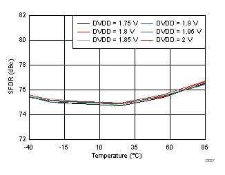
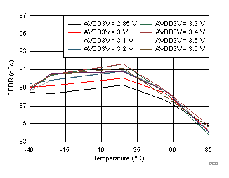
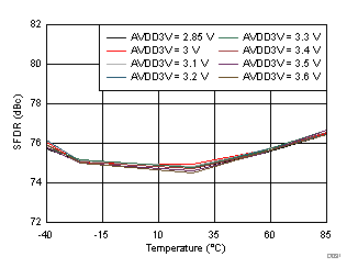
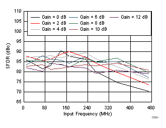
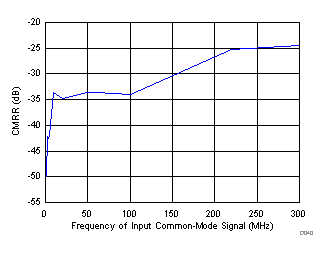
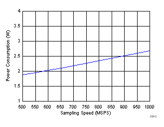
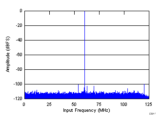
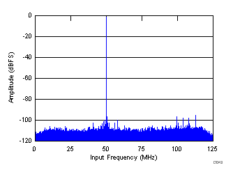
typical values are at TA = 25°C, full temperature range is from TMIN = –40°C to TMAX = 85°C, ADC sampling rate = 1.0 GSPS, 50% clock duty cycle, AVDD3V = 3.0 V, AVDD = DVDD = 1.9 V, IOVDD = 1.15 V, and –1-dBFS differential input (unless otherwise noted)
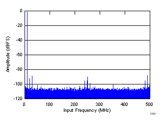
ADS54J60 D001_SBAS706.gif
SNR = 71 dBFS; SFDR = 86 dBc;
IL spur = 94 dBc; non HD2, HD3 spur = 89 dBc
Figure 3. FFT for 10-MHz Input Signal
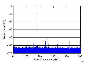
ADS54J60 D003_SBAS706.gif
SNR = 69.8 dBFS; SFDR = 88 dBc;
IL spur = 86 dBc; non HD2, HD3 spur = 89 dBc
Figure 5. FFT for 170-MHz Input Signal
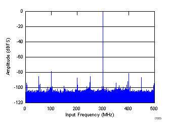
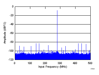
ADS54J60 D005_SBAS706.gif
SNR = 68 dBFS; SFDR = 77 dBc;
IL spur = 84 dBc; non HD2, HD3 spur = 85 dBc
Figure 7. FFT for 300-MHz Input Signal
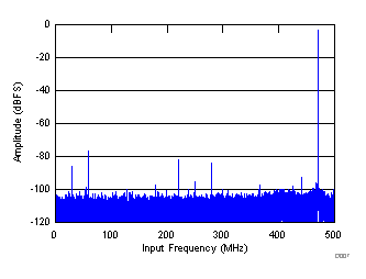
ADS54J60 D007_SBAS706.gif
SNR = 67.9 dBFS; SFDR = 74 dBc;
IL spur = 82 dBc; non HD2, HD3 spur = 89 dBc
Figure 9. FFT for 470-MHz Input Signal at –3 dBFS
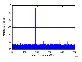
ADS54J60 D008_SBAS706.gif
fIN1 = 185 MHz, fIN2 = 190 MHz, each tone at –7 dBFS,
IMD3 = 88 dBFS
Figure 11. FFT for Two-Tone Input Signal (–7 dBFS)
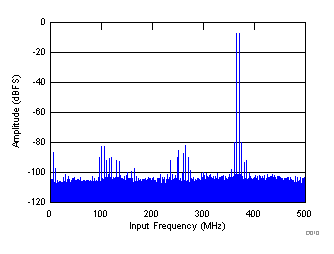
ADS54J60 D010_SBAS706.gif
fIN1 = 365 MHz, fIN2 = 370 MHz, each tone at –7 dBFS,
IMD3 = 80 dBFS
Figure 13. FFT for Two-Tone Input Signal (–7 dBFS)
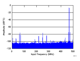
ADS54J60 D012_SBAS706.gif
fIN1 = 465 MHz, fIN2 = 470 MHz, each tone at –7 dBFS,
IMD3 = 75 dBFS
Figure 15. FFT for Two-Tone Input Signal (–7 dBFS)
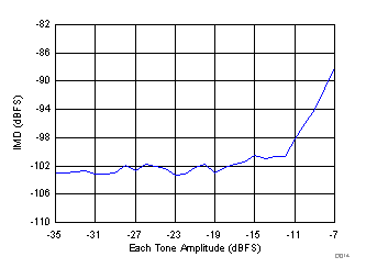
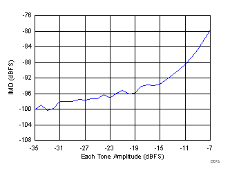
ADS54J60 D014_SBAS706.gif
fIN1 = 185 MHz, fIN2 = 190 MHz
Figure 17. Intermodulation Distortion vs
Input Tone Amplitude
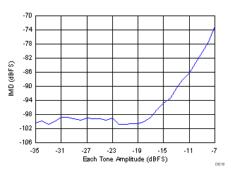
ADS54J60 D016_SBAS706.gif
fIN1 = 465 MHz, fIN2 = 470 MHz
Figure 19. Intermodulation Distortion vs
Input Tone Amplitude
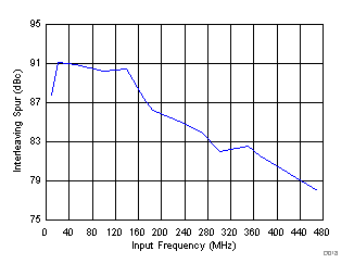
ADS54J60 D018_SBAS706.gif
Figure 21. IL Spur vs Input Frequency
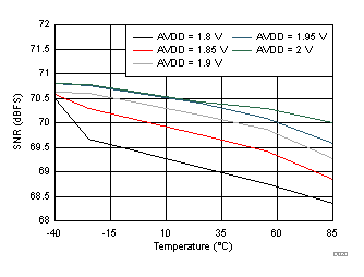
ADS54J60 D020_SBAS706.gif
fIN = 170 MHz
Figure 23. Signal-to-Noise Ratio vs
AVDD Supply and Temperature
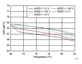
ADS54J60 D022_SBAS706.gif
fIN = 350 MHz
Figure 25. Signal-to-Noise Ratio vs
AVDD Supply and Temperature
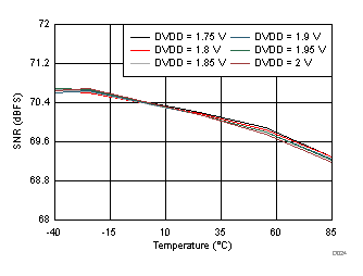
ADS54J60 D024_SBAS706.gif
fIN = 170 MHz
Figure 27. Signal-to-Noise Ratio vs
DVDD Supply and Temperature
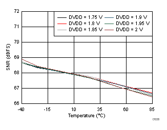
ADS54J60 D026_SBAS706.gif
fIN = 350 MHz
Figure 29. Signal-to-Noise Ratio vs
DVDD Supply and Temperature
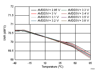
ADS54J60 D028_SBAS706.gif
fIN = 170 MHz
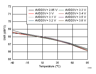
Figure 31. Signal-to-Noise Ratio vs
AVDD3V Supply and Temperature
ADS54J60 D030_SBAS706.gif
fIN = 350 MHz
Figure 33. Signal-to-Noise Ratio vs
AVDD3V Supply and Temperature
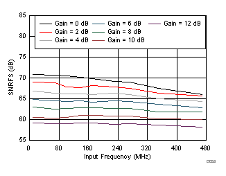
ADS54J60 D053_SBAS706.gif
Figure 35. Signal-to-Noise Ratio vs
Gain and Input Frequency
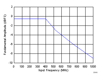
ADS54J60 D046_SBAS706.gif
Figure 37. Maximum Supported Amplitude vs Frequency
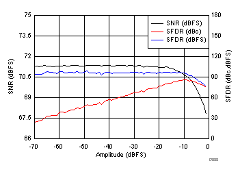
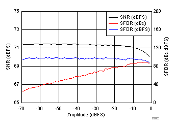
ADS54J60 D033_SBAS706.gif
fIN = 350 MHz
Figure 39. Performance vs Input Amplitude
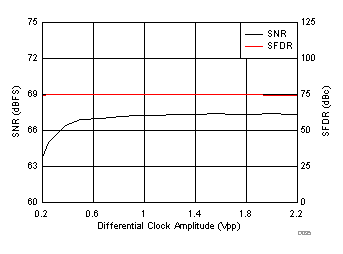
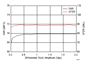
ADS54J60 D035_SBAS706.gif
fIN = 350 MHz
Figure 41. Performance vs Sampling Clock Amplitude
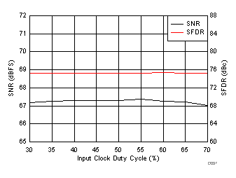
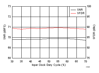
ADS54J60 D037_SBAS706.gif
fIN = 350 MHz
Figure 43. Performance vs Clock Duty Cycle
ADS54J60 D039_SBAS706.gif
fIN = 170 MHz , AIN = –1 dBFS, SINAD = 67 dBFS,
SFDR = 79 dBc, fPSRR = 5 MHz, APSRR = 25 mVPP,
amplitude of fIN – fPSRR = –74 dBFS,
amplitude of fIN + fPSRR = –76 dBFS
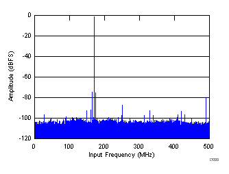
Figure 45. Power-Supply Rejection Ratio FFT for
Test Signals on the AVDD Supply
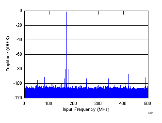
ADS54J60 D041_SBAS706.gif
fIN = 170 MHz , AIN = –1 dBFS, fCMRR = 5 MHz, ACMRR = 50 mVPP, SINAD = 69.1 dBFS, SFDR = 86 dBc,
amplitude of fIN ± fCMRR= –80 dBFS
Figure 47. Common-Mode Rejection Ratio FFT
ADS54J60 D045_SBAS706.gif
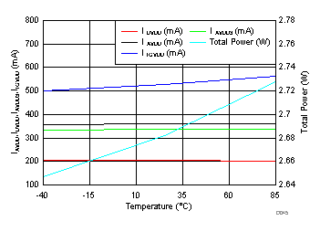
Figure 49. Power vs Temperature
ADS54J60 D048_SBAS706.gif
SNR = 75.2 dBFS, SFDR = 90 dBc
Figure 51. FFT for 170-MHz Input Signal in
Decimate-by-4 Mode
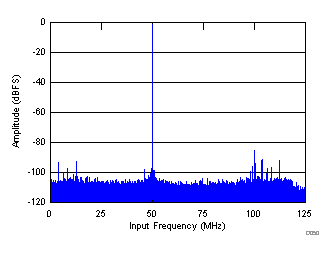
ADS54J60 D050_SBAS706.gif
SNR = 69.6 dBFS, SFDR = 84 dBc
Figure 53. FFT for 450-MHz Input Signal in
Decimate-by-4 Mode
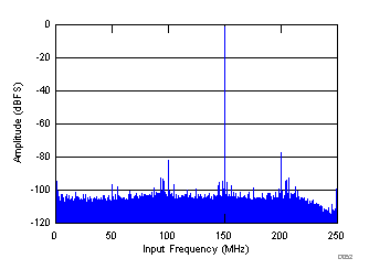
ADS54J60 D052_SBAS706.gif
SNR = 68.3 dBFS, SFDR = 80 dBc
Figure 55. FFT for 350-MHz Input Signal in
Decimate-by-2 Mode
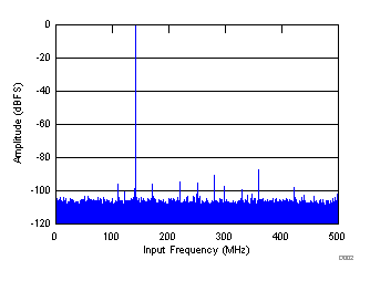
ADS54J60 D002_SBAS706.gif
SNR = 70.3 dBFS; SFDR = 90 dBc;
IL spur = 95 dBc; non HD2, HD3 spur = 94 dBc
Figure 4. FFT for 140-MHz Input Signal
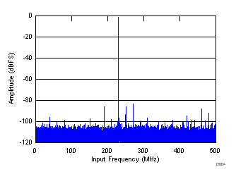
ADS54J60 D004_SBAS706.gif
SNR = 68.9 dBFS; SFDR = 85 dBc;
IL spur = 85 dBc; non HD2, HD3 spur = 86 dBc
Figure 6. FFT for 230-MHz Input Signal
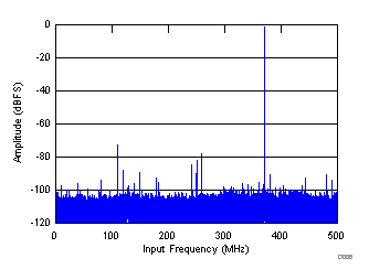
ADS54J60 D006_SBAS706.gif
SNR = 66.7 dBFS; SFDR = 71 dBc;
IL spur = 87 dBc; non HD2, HD3 spur = 78 dBc
Figure 8. FFT for 370-MHz Input Signal
ADS54J60 FFT for 720MHz.gif
SNR = 66.3 dBFS, SINAD = 65.3 dBFS, THD = 70 dBc,
IL spur = 84 dBc, SFDR = 73 dBc, non HD2, HD3 spur = 90 dBFS
Figure 10. FFT for 720-MHz Input Signal at –6 dBFS
ADS54J60 D009_SBAS706.gif
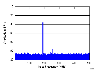
fIN1 = 185 MHz, fIN2 = 190 MHz, each tone at –36 dBFS,
IMD3 = 106 dBFS
Figure 12. FFT for Two-Tone Input Signal (–36 dBFS)
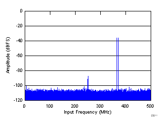
ADS54J60 D011_SBAS706.gif
fIN1 = 365 MHz, fIN2 = 370 MHz, each tone at –36 dBFS,
IMD3 = 105 dBFS
Figure 14. FFT for Two-Tone Input Signal (–36 dBFS)
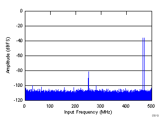
ADS54J60 D013_SBAS706.gif
fIN1 = 465 MHz, fIN2 = 470 MHz, each tone at –36 dBFS,
IMD3 = 106 dBFS
Figure 16. FFT for Two-Tone Input Signal (–36 dBFS)
ADS54J60 D015_SBAS706.gif
fIN1 = 365 MHz, fIN2 = 370 MHz
Figure 18. Intermodulation Distortion vs
Input Tone Amplitude
ADS54J60 D043_SBAS706.gif
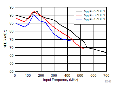
Figure 20. Spurious-Free Dynamic Range vs
Input Frequency
ADS54J60 D042_SBAS706.gif
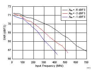
Figure 22. Signal-to-Noise Ratio vs Input Frequency
ADS54J60 D021_SBAS706.gif
fIN = 170 MHz
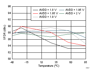
Figure 24. Spurious-Free Dynamic Range vs
AVDD Supply and Temperature
ADS54J60 D023_SBAS706.gif
fIN = 350 MHz
Figure 26. Spurious-Free Dynamic Range vs
AVDD Supply and Temperature
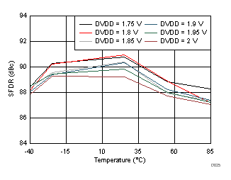
ADS54J60 D025_SBAS706.gif
fIN = 170 MHz
Figure 28. Spurious-Free Dynamic Range vs
DVDD Supply and Temperature
ADS54J60 D027_SBAS706.gif
fIN = 350 MHz
Figure 30. Spurious-Free Dynamic Range vs
DVDD Supply and Temperature
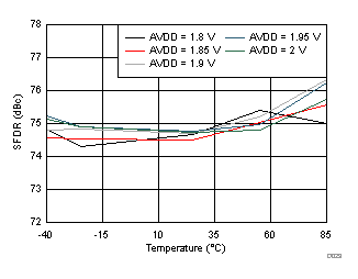
ADS54J60 D029_SBAS706.gif
fIN = 170 MHz
Figure 32. Spurious-Free Dynamic Range vs
AVDD3V Supply and Temperature
ADS54J60 D031_SBAS706.gif
fIN = 350 MHz
Figure 34. Spurious-Free Dynamic Range vs
AVDD3V Supply and Temperature
ADS54J60 D054_SBAS706.gif
Figure 36. Spurious-Free Dynamic Range vs
Gain and Input Frequency
ADS54J60 D032_SBAS706.gif
fIN = 170 MHz
Figure 38. Performance vs Input Amplitude
ADS54J60 D034_SBAS706.gif
fIN = 170 MHz
Figure 40. Performance vs Sampling Clock Amplitude
ADS54J60 D036_SBAS706.gif
fIN = 170 MHz
Figure 42. Performance vs Clock Duty Cycle
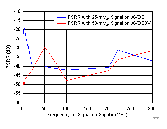
ADS54J60 D038_SBAS706.gif
fIN = 170 MHz
Figure 44. Power-Supply Rejection Ratio vs
Test Signal Frequency
ADS54J60 D040_SBAS706.gif
fIN = 170 MHz
Figure 46. Common-Mode Rejection Ratio vs
Test Signal Frequency
ADS54J60 D044_SBAS706.gif
Figure 48. Power vs Sampling Speed
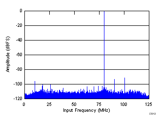
ADS54J60 D047_SBAS706.gif
SNR = 76.4 dBFS, SFDR = 99 dBc
Figure 50. FFT for 60-MHz Input Signal in
Decimate-by-4 Mode
ADS54J60 D049_SBAS706.gif
SNR = 72.8 dBFS, SFDR = 91 dBc
Figure 52. FFT for 300-MHz Input Signal in
Decimate-by-4 Mode
ADS54J60 D051_SBAS706.gif
SNR = 71.9 dBFS, SFDR = 89 dBc
Figure 54. FFT for 170-MHz Input Signal in
Decimate-by-2 Mode