JAJSH87D April 2015 – April 2019 ADS54J60
PRODUCTION DATA.
- 1 特長
- 2 アプリケーション
- 3 概要
- 4 改訂履歴
- 5 Device Comparison Table
- 6 Pin Configuration and Functions
- 7 Specifications
-
8 Detailed Description
- 8.1 Overview
- 8.2 Functional Block Diagram
- 8.3 Feature Description
- 8.4 Device Functional Modes
- 8.5
Register Maps
- 8.5.1 Example Register Writes
- 8.5.2
Register Descriptions
- 8.5.2.1 General Registers
- 8.5.2.2
Master Page (080h) Registers
- 8.5.2.2.1 Register 20h (address = 20h), Master Page (080h)
- 8.5.2.2.2 Register 21h (address = 21h), Master Page (080h)
- 8.5.2.2.3 Register 23h (address = 23h), Master Page (080h)
- 8.5.2.2.4 Register 24h (address = 24h), Master Page (080h)
- 8.5.2.2.5 Register 26h (address = 26h), Master Page (080h)
- 8.5.2.2.6 Register 4Fh (address = 4Fh), Master Page (080h)
- 8.5.2.2.7 Register 53h (address = 53h), Master Page (080h)
- 8.5.2.2.8 Register 54h (address = 54h), Master Page (080h)
- 8.5.2.2.9 Register 55h (address = 55h), Master Page (080h)
- 8.5.2.2.10 Register 59h (address = 59h), Master Page (080h)
- 8.5.2.3 ADC Page (0Fh) Register
- 8.5.2.4
Main Digital Page (6800h) Registers
- 8.5.2.4.1 Register 0h (address = 0h), Main Digital Page (6800h)
- 8.5.2.4.2 Register 41h (address = 41h), Main Digital Page (6800h)
- 8.5.2.4.3 Register 42h (address = 42h), Main Digital Page (6800h)
- 8.5.2.4.4 Register 43h (address = 43h), Main Digital Page (6800h)
- 8.5.2.4.5 Register 44h (address = 44h), Main Digital Page (6800h)
- 8.5.2.4.6 Register 4Bh (address = 4Bh), Main Digital Page (6800h)
- 8.5.2.4.7 Register 4Dh (address = 4Dh), Main Digital Page (6800h)
- 8.5.2.4.8 Register 4Eh (address = 4Eh), Main Digital Page (6800h)
- 8.5.2.4.9 Register 52h (address = 52h), Main Digital Page (6800h)
- 8.5.2.4.10 Register 72h (address = 72h), Main Digital Page (6800h)
- 8.5.2.4.11 Register ABh (address = ABh), Main Digital Page (6800h)
- 8.5.2.4.12 Register ADh (address = ADh), Main Digital Page (6800h)
- 8.5.2.4.13 Register F7h (address = F7h), Main Digital Page (6800h)
- 8.5.2.5
JESD Digital Page (6900h) Registers
- 8.5.2.5.1 Register 0h (address = 0h), JESD Digital Page (6900h)
- 8.5.2.5.2 Register 1h (address = 1h), JESD Digital Page (6900h)
- 8.5.2.5.3 Register 2h (address = 2h), JESD Digital Page (6900h)
- 8.5.2.5.4 Register 3h (address = 3h), JESD Digital Page (6900h)
- 8.5.2.5.5 Register 5h (address = 5h), JESD Digital Page (6900h)
- 8.5.2.5.6 Register 6h (address = 6h), JESD Digital Page (6900h)
- 8.5.2.5.7 Register 7h (address = 7h), JESD Digital Page (6900h)
- 8.5.2.5.8 Register 16h (address = 16h), JESD Digital Page (6900h)
- 8.5.2.5.9 Register 31h (address = 31h), JESD Digital Page (6900h)
- 8.5.2.5.10 Register 32h (address = 32h), JESD Digital Page (6900h)
- 8.5.2.6
JESD Analog Page (6A00h) Registers
- 8.5.2.6.1 Register 12h (address = 12h), JESD Analog Page (6A00h)
- 8.5.2.6.2 Registers 13h-15h (address = 13h-15h), JESD Analog Page (6A00h)
- 8.5.2.6.3 Register 16h (address = 16h), JESD Analog Page (6A00h)
- 8.5.2.6.4 Register 17h (address = 17h), JESD Analog Page (6A00h)
- 8.5.2.6.5 Register 1Ah (address = 1Ah), JESD Analog Page (6A00h)
- 8.5.2.6.6 Register 1Bh (address = 1Bh), JESD Analog Page (6A00h)
- 8.5.2.7
Offset Read Page (JESD BANK PAGE SEL = 6100h, JESD BANK PAGE SEL1 = 0000h) Registers
- 8.5.2.7.1 Register 068h (address = 068h), Offset Read Page
- 8.5.2.7.2 Register 069h (address = 069h), Offset Read Page
- 8.5.2.7.3 Registers 074h, 076h, 078h, 7Ah (address = 074h, 076h, 078h, 7Ah), Offset Read Page
- 8.5.2.7.4 Registers 075h, 077h, 079h, 7Bh (address = 075h, 077h, 079h, 7Bh), Offset Read Page
- 8.5.2.8 Offset Load Page (JESD BANK PAGE SEL= 6100h, JESD BANK PAGE SEL1 = 0500h) Registers
- 9 Application and Implementation
- 10Power Supply Recommendations
- 11Layout
- 12デバイスおよびドキュメントのサポート
- 13メカニカル、パッケージ、および注文情報
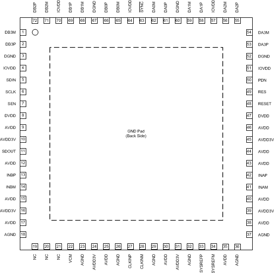
6 Pin Configuration and Functions
RMP Package
72-Pin VQFNP
Top View
