JAJSPK6B December 2015 – January 2023 ADS54J66
PRODUCTION DATA
- 1 特長
- 2 アプリケーション
- 3 概要
- 4 Revision History
- 5 Pin Configuration and Functions
-
6 Specifications
- 6.1 Absolute Maximum Ratings
- 6.2 ESD Ratings
- 6.3 Recommended Operating Conditions
- 6.4 Thermal Information
- 6.5 Electrical Characteristics
- 6.6 AC Performance
- 6.7 Digital Characteristics
- 6.8 Timing Requirements
- 6.9 Typical Characteristics: General (DDC Mode-8)
- 6.10 Typical Characteristics: Mode 2
- 6.11 Typical Characteristics: Mode 0
-
7 Detailed Description
- 7.1 Overview
- 7.2 Functional Block Diagram
- 7.3 Feature Description
- 7.4
Device Functional Modes
- 7.4.1 Digital Features
- 7.4.2 Mode 0, Decimation-by-2 with IQ Outputs for up to 220 MHz of IQ Bandwidth
- 7.4.3 Mode 2, Decimation-by-2 for up to 110 MHz of Real Bandwidth
- 7.4.4 Modes 4 and 7, Decimation-by-2 with Real Outputs for up to 110 MHz of Bandwidth
- 7.4.5 Mode 5, Decimation-by-2 with IQ Outputs for up to 110 MHz of IQ Bandwidth
- 7.4.6 Mode 6, Decimation-by-4 with IQ Outputs for up to 110 MHz of IQ Bandwidth
- 7.4.7 Overrange Indication
- 7.4.8 Power-Down Mode
- 7.5 Programming
- 7.6
Register Maps
- 7.6.1 Detailed Register Information
- 7.6.2 Example Register Writes
- 7.6.3
Register Descriptions
- 7.6.3.1 General Registers
- 7.6.3.2
Master Page (80h)
- 7.6.3.2.1 Register 20h (address = 20h) [reset = 0h], Master Page (080h)
- 7.6.3.2.2 Register 21h (address = 21h) [reset = 0h], Master Page (080h)
- 7.6.3.2.3 Register 23h (address = 23h), Master Page (080h)
- 7.6.3.2.4 Register 24h (address = 24h) [reset = 0h], Master Page (080h)
- 7.6.3.2.5 Register 26h (address = 26h), Master Page (080h)
- 7.6.3.2.6 Register 3Ah (address = 3Ah) [reset = 0h], Master Page (80h)
- 7.6.3.2.7 Register 39h (address = 39h) [reset = 0h], Master Page (80h)
- 7.6.3.2.8 Register 53h (address = 53h) [reset = 0h], Master Page (80h)
- 7.6.3.2.9 Register 54h (address = 54h) [reset = 0h], Master Page (80h)
- 7.6.3.2.10 Register 55h (address = 55h) [reset = 0h], Master Page (80h)
- 7.6.3.2.11 Register 56h (address = 56h) [reset = 0h], Master Page (80h)
- 7.6.3.2.12 Register 59h (address = 59h) [reset = 0h], Master Page (80h)
- 7.6.3.3
ADC Page (0Fh)
- 7.6.3.3.1 Register 5Fh (address = 5Fh) [reset = 0h], ADC Page (0Fh)
- 7.6.3.3.2 Register 60h (address = 60h) [reset = 0h], ADC Page (0Fh)
- 7.6.3.3.3 Register 61h (address = 61h) [reset = 0h], ADC Page (0Fh)
- 7.6.3.3.4 Register 6Ch (address = 6Ch) [reset = 0h], ADC Page (0Fh)
- 7.6.3.3.5 Register 6Dh (address = 6Dh) [reset = 0h], ADC Page (0Fh)
- 7.6.3.3.6 Register 74h (address = 74h) [reset = 0h], ADC Page (0Fh)
- 7.6.3.3.7 Register 75h (address = 75h) [reset = 0h], ADC Page (0Fh)
- 7.6.3.3.8 Register 76h (address = 76h) [reset = 0h], ADC Page (0Fh)
- 7.6.3.3.9 Register 77h (address = 77h) [reset = 0h], ADC Page (0Fh)
- 7.6.3.3.10 Register 78h (address = 78h) [reset = 0h], ADC Page (0Fh)
- 7.6.3.4 Interleaving Engine Page (6100h)
- 7.6.3.5 Decimation Filter Page (6141h) Registers
- 7.6.3.6
Main Digital Page (6800h) Registers
- 7.6.3.6.1 Register 0h (address = 0h) [reset = 0h], Main Digital Page (6800h)
- 7.6.3.6.2 Register 42h (address = 42h) [reset = 0h], Main Digital Page (6800h)
- 7.6.3.6.3 Register 4Eh (address = 4Eh) [reset = 0h], Main Digital Page (6800h)
- 7.6.3.6.4 Register ABh (address = ABh) [reset = 0h], Main Digital Page (6800h)
- 7.6.3.6.5 Register ADh (address = ADh) [reset = 0h], Main Digital Page (6800h)
- 7.6.3.6.6 Register F7h (address = F7h) [reset = 0h], Main Digital Page (68h)
- 7.6.3.7
JESD Digital Page (6900h) Registers
- 7.6.3.7.1 Register 0h (address = 0h) [reset = 0h], JESD Digital Page (6900h)
- 7.6.3.7.2 Register 1h (address = 1h) [reset = 0h], JESD Digital Page (6900h)
- 7.6.3.7.3 Register 2h (address = 2h) [reset = 0h], JESD Digital Page (6900h)
- 7.6.3.7.4 Register 3h (address = 3h) [reset = 0h], JESD Digital Page (6900h)
- 7.6.3.7.5 Register 5h (address = 5h) [reset = 0h], JESD Digital Page (6900h)
- 7.6.3.7.6 Register 6h (address = 6h) [reset = 0h], JESD Digital Page (6900h)
- 7.6.3.7.7 Register 21h (address = 21h) [reset = 0h], JESD Digital Page (6900h)
- 7.6.3.7.8 Register 22h (address = 22h) [reset = 0h], JESD Digital Page (6900h)
- 7.6.3.8
JESD Analog Page (6A00h) Register
- 7.6.3.8.1 Register 12h, 13h (address 12h, 13h) [reset = 0h], JESD Analog Page (6Ah)
- 7.6.3.8.2 Register 16h (address = 16h) [reset = 0h], JESD Analog Page (6A00h)
- 7.6.3.8.3 Register 17h (address = 17h) [reset = 0h], JESD Analog Page (6A00h)
- 7.6.3.8.4 Register 1Bh (address = 1Bh) [reset = 0h], JESD Analog Page (6A00h)
- 8 Application Information Disclaimer
- 9 Device and Documentation Support
- 10Mechanical, Packaging, and Orderable Information
8.3.1 Power Sequencing and Initialization
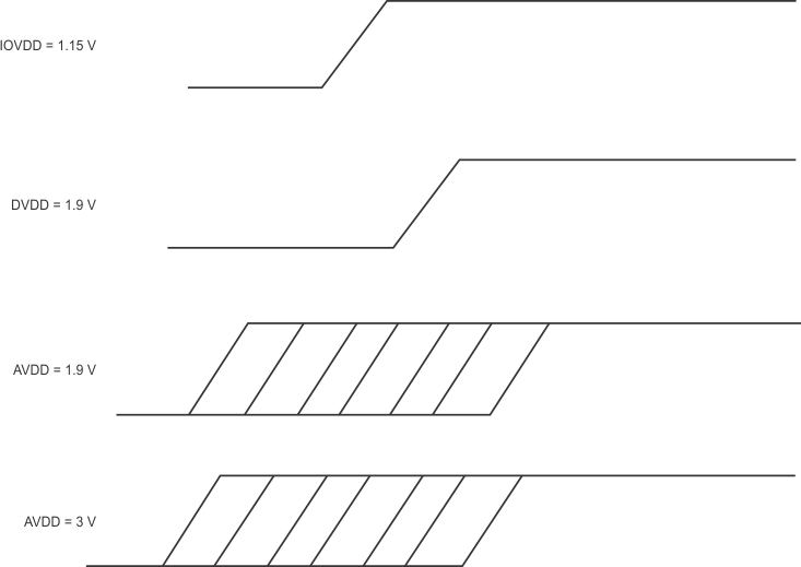
Figure 8-9 shows the suggested power-up sequencing for the device. The 1.15-V IOVDD supply must rise before the 1.9-V DVDD supply. If the 1.9-V DVDD supply rises before the 1.15-V IOVDD supply, then the internal default register settings may not load properly. The other supplies (the 3-V AVDD3V and the 1.9-V AVDD), can come up in any order during the power sequence. The power supplies can ramp up at any rate and there is no hard requirement for the time delay between IOVDD ramp up to DVDD ramp-up (can be in orders of microseconds but is recommend to be a few milliseconds).
 Figure 8-9 Power Sequencing for the
ADS54J66 Device