-
ADS556x 16-Bit, 40 and 80 MSPS ADCs With DDR LVDS and CMOS Outputs
- 1 Features
- 2 Applications
- 3 Description
- 4 Revision History
- 5 Pin Configuration and Functions
-
6 Specifications
- 6.1 Absolute Maximum Ratings
- 6.2 ESD Ratings
- 6.3 Recommended Operating Conditions
- 6.4 Thermal Information
- 6.5 Electrical Characteristics
- 6.6 AC Electrical Characteristics for ADS5560 Fs = 40 MSPS
- 6.7 AC Electrical Characteristics for ADS5562, Fs = 80 MSPS
- 6.8 Electrical Characteristics for ADS5562
- 6.9 Electrical Characteristics for ADS5560
- 6.10 Digital Characteristics
- 6.11 Timing Characteristics for LVDS and CMOS Modes
- 6.12 Serial Interface Timing Characteristics
- 6.13 Reset Timing
- 6.14 Timing Characteristics at Lower Sampling Frequencies
- 6.15 Typical Characteristics
- 7 Detailed Description
- 8 Application and Implementation
- 9 Power Supply Recommendations
- 10Layout
- 11Device and Documentation Support
- 12Mechanical, Packaging, and Orderable Information
- IMPORTANT NOTICE
パッケージ・オプション
メカニカル・データ(パッケージ|ピン)
- RGZ|48
サーマルパッド・メカニカル・データ
- RGZ|48
発注情報
ADS556x 16-Bit, 40 and 80 MSPS ADCs With DDR LVDS and CMOS Outputs
1 Features
- 16-Bit Resolution
- Maximum Sample Rate:
- ADS5562: 80 MSPS
- ADS5560: 40 MSPS
- Total Power:
- 865 mW at 80 MSPS
- 674 mW at 40 MSPS
- No Missing Codes
- High SNR: 84 dBFS (3 MHz IF)
- SFDR: 85 dBc (3 MHz IF)
- Low-Frequency Noise Suppression Mode
- Programmable Fine Gain, 1-dB steps Until 6-dB Maximum Gain
- Double Data-Rate (DDR) LVDS and Parallel CMOS Output Options
- Internal and External Reference Support
- 3.3-V Analog and Digital Supply
- Pin-for-Pin With ADS5547 Family
- 48-VQFN Package (7.00 mm × 7.00 mm)
2 Applications
- Medical Imaging, MRI
- Wireless Communications Infrastructure
- Software Defined Radio
- Test and Measurement Instrumentation
- High Definition Video
3 Description
The ADS556x is a high-performance 16-bit family of ADCs with sampling rates up to 80 MSPS. The device supports very-high SNR for input frequencies in the first Nyquist zone. The device includes a low-frequency noise suppression mode that improves the noise from DC to about 1 MHz.
In addition to high performance, the device offers several flexible features such as output interface (either Double Data Rate [DDR] LVDS or parallel CMOS) and fine gain in 1-dB steps until 6-dB maximum gain.
Innovative techniques, such as DDR LVDS and an internal reference that does not require external decoupling capacitors, have been used to achieve significant savings in pin count. This innovation results in a compact 7-mm × 7-mm 48-pin VQFN package.
The device can be put in an external reference mode, where the VCM pin behaves as the external reference input. For applications where power is important, the ADS556x device offers power down modes and automatic power scaling at lower sample rates.
The device is specified over the industrial temperature range of –40°C to 85°C.
Device Information(1)
| PART NUMBER | PACKAGE | BODY SIZE (NOM) |
|---|---|---|
| ADS5560 | VQFN (48) | 7.00 mm × 7.00 mm |
| ADS5562 |
- For all available packages, see the orderable addendum at the end of the data sheet.
Block Diagram
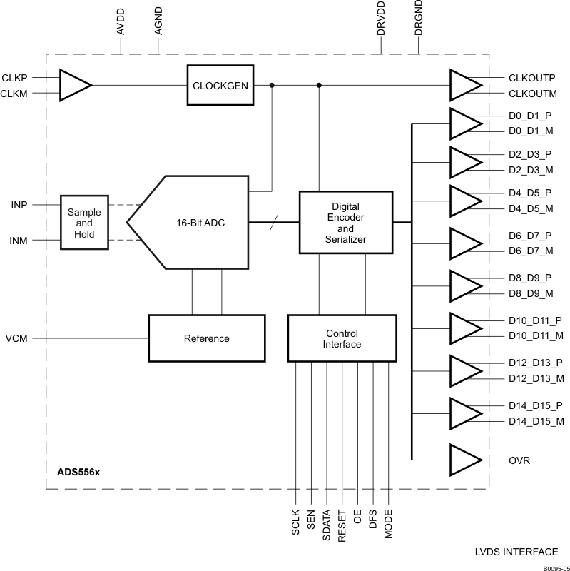
4 Revision History
Changes from A Revision (May 2012) to B Revision
- Added ESD Ratings table, Feature Description section, Device Functional Modes, Application and Implementation section, Power Supply Recommendations section, Layout section, Device and Documentation Support section, and Mechanical, Packaging, and Orderable Information section.Go
Changes from * Revision (May 2008) to A Revision
- Changed Programmable Fine Gain in FEATURESGo
- Added maximum gain to end of second paragraph of DESCRIPTIONGo
- Changed Voltage between AVDD to DRVDD to Voltage between AVDD and DRVDD in ABS MAX RATINGSGo
- Added Voltage applied to analog input pins, INP, INM in ABS MAX RATINGSGo
- Added Voltage applied to analog input pins, CLKP, CLKM, MODE in ABS MAX RATINGSGo
- Added Voltage applied to analog input pins, RESET, SCLK, SDATA, SEN, OE, DFS in ABS MAX RATINGSGo
- Changed boundary between DEFAULT SPEED mode and LOW SPEED mode from 30 MSPS to 25 MSPS in RECOMMENDED OPERATING CONDITIONS Go
- Changed tho to th in header row of Timing Characteristics at Lower Sampling FrequenciesGo
- Added text to Note regarding RESET pulse requirement in Figure 1Go
- Added 32k Point FFT to TYPICAL CHARACTERISTICS section conditions Go
- Changed Figure 48Go
- Added text to end of Programmable Fine Gain sectionGo
- Added (Serial Interface Mode) to Table 1 titleGo
- Changed LOW SPEED mode boundary from 30 MSPS to 25 MSPS in Low Sampling Frequency Operation sectionGo
- Added text to Clock Input sectionGo
- Changed Clock Input section paragraphs and 4 illustrationsGo
- Added (of width greater than 10ns) in USING SERIAL INTERFACE PROGRAMMING ONLY sectionGo
- Added to Priority last row in Table 3 Go
- Changed Parallel Interface Control description for SCLK Control Pin, (SCLK = 0, 3dB gain; SCLK = DRVDD, 1 dB gain) in Table 4Go
- Changed first pargraph in SERIAL INTERFACE sectionGo
- Added text to Table 9 NoteGo
- Changed Fs > 30 MSPS to Fs > 25 MSPS in <LOW SPEED> Go
5 Pin Configuration and Functions

Pin Functions - LVDS Mode
| PIN | I/O | DESCRIPTION | |
|---|---|---|---|
| NO. | NAME | ||
| 9, 12, 14, 17, 19, 25 | AGND | I | Analog ground |
| 8, 18, 20, 22, 24, 26 |
AVDD | I | Analog power supply |
| 4 | CLKOUTM | O | Differential output clock, complement |
| 5 | CLKOUTP | O | Differential output clock, true |
| 10 | CLKP | I | Differential clock input |
| 11 | CLKM | ||
| 31 | D0_D1_M | O | Differential output data D0 and D1 multiplexed, complement. |
| 32 | D0_D1_P | O | Differential output data D0 and D1 multiplexed, true |
| 43 | D10_D11_M | O | Differential output data D10 and D11 multiplexed, complement |
| 44 | D10_D11_P | O | Differential output data D10 and D11 multiplexed, true |
| 45 | D12_D13_M | O | Differential output data D12 and D13 multiplexed, complement |
| 46 | D12_D13_P | O | Differential output data D12 and D13 multiplexed, true |
| 47 | D14_D15_M | O | Differential output data D14 and D15 multiplexed, complement |
| 48 | D14_D15_P | O | Differential output data D14 and D15 multiplexed, true |
| 33 | D2_D3_M | O | Differential output data D2 and D3 multiplexed, complement |
| 34 | D2_D3_P | O | Differential output data D2 and D3 multiplexed, true |
| 37 | D4_D5_M | O | Differential output data D4 and D5 multiplexed, complement |
| 38 | D4_D5_P | O | Differential output data D4 and D5 multiplexed, true |
| 39 | D6_D7_M | O | Differential output data D6 and D7 multiplexed, complement |
| 40 | D6_D7_P | O | Differential output data D6 and D7 multiplexed, true |
| 41 | D8_D9_M | O | Differential output data D8 and D9 multiplexed, complement |
| 42 | D8_D9_P | O | Differential output data D8 and D9 multiplexed, true |
| 6 | DFS | I | Data Format Select input. This pin sets the DATA FORMAT (2s complement or Offset binary) and the LVDS/CMOS output mode type. See Table 7 for detailed information. The pin has an internal 100-kΩ pulldown resistor to DRGND. |
| 1, 36 | DRGND | I | Digital and output buffer ground |
| 2, 35 | DRVDD | I | Digital and output buffer supply |
| 15 | INP | I | Differential analog input |
| 16 | INM | ||
| 23 | MODE | I | Mode select input. This pin selects the Internal or External reference mode. See Table 8 for detailed information. The pin has an internal 100-kΩ pulldown resistor to AGND. |
| 21 | NC | — | Do not connect |
| 7 | OE | I | Output buffer enable input, active high. The pin has an internal 100-kΩ pullup resistor to DRVDD. |
| 3 | OVR | O | Out-of-range indicator, CMOS level signal |
| 30 | RESET | I | Serial interface reset input. When using the serial interface, the user should apply a high-going pulse on this pin to reset the internal registers. When the serial interface is not used, the user should tie RESET permanently high. (SCLK, SDATA and SEN can be used as parallel pin controls). The pin has an internal 100-kΩ pulldown resistor to DRGND. |
| 29 | SCLK | I | This pin functions as serial interface clock input when RESET is low. It functions as LOW SPEED MODE control when RESET is tied high. See Table 4 for detailed information. The pin has an internal 100-kΩ pulldown resistor to DRGND. |
| 28 | SDATA | I | This pin functions as serial interface data input when RESET is low. It functions as STANDBY control pin when RESET is tied high. See Table 5 for detailed information. The pin has an internal 100-kΩ pulldown resistor to DRGND. |
| 27 | SEN | I | This pin functions as serial interface enable input when RESET is low. It functions as CLKOUT edge programmability when RESET is tied high. See Table 6 for detailed information. The pin has an internal 100-kΩ pullup resistor to DRVDD. |
| 13 | VCM | I/O | Internal reference mode – Common-mode voltage output. External reference mode – Reference input. The voltage forced on this pin sets the internal reference. |
| — | PAD | — | Connect the PAD to the ground plane. See the Exposed Thermal Pad section. |

Pin Functions - CMOS Mode
| PIN | I/O | DESCRIPTION | |
|---|---|---|---|
| NO. | NAME | ||
| 9, 12, 14, 17, 19, 25 | AGND | I | Analog ground |
| 8, 18, 20, 22, 24, 26 |
AVDD | I | Analog power supply |
| 5 | CLKOUT | O | CMOS output clock |
| 10 | CLKP | I | Differential clock input |
| 11 | CLKM | ||
| 31 | D0 | O | CMOS output data D0 |
| 32 | D1 | O | CMOS output data D1 |
| 43 | D10 | O | CMOS output data D10 |
| 44 | D11 | O | CMOS output data D11 |
| 45 | D12 | O | CMOS output data D12 |
| 46 | D13 | O | CMOS output data D13 |
| 47 | D14 | O | CMOS output data D14 |
| 48 | D15 | O | CMOS output data D15 |
| 33 | D2 | O | CMOS output data D2 |
| 34 | D3 | O | CMOS output data D3 |
| 37 | D4 | O | CMOS output data D4 |
| 38 | D5 | O | CMOS output data D5 |
| 39 | D6 | O | CMOS output data D6 |
| 40 | D7 | O | CMOS output data D7 |
| 41 | D8 | O | CMOS output data D8 |
| 42 | D9 | O | CMOS output data D9 |
| 6 | DFS | I | Data Format Select input. This pin sets the DATA FORMAT (2s complement or Offset binary) and the LVDS/CMOS output mode type. See Table 7 for detailed information. The pin has an internal 100-kΩ pulldown resistor to DRGND. |
| 1, 36 | DRGND | I | Digital and output buffer ground |
| 2, 35 | DRVDD | I | Digital and output buffer supply |
| 15 | INP | I | Differential analog input |
| 16 | INM | ||
| 23 | MODE | I | Mode select input. This pin selects the Internal or External reference mode. See Table 8 for detailed information. The pin has an internal 100-kΩ pulldown resistor to AGND. |
| 21 | NC | — | Do not connect |
| 7 | OE | I | Output buffer enable input, active high. The pin has an internal 100-kΩ pullup resistor to DRVDD. |
| 3 | OVR | O | Out-of-range indicator, CMOS level signal |
| 30 | RESET | I | Serial interface reset input. When using the serial interface, the user should apply a high-going pulse on this pin to reset the internal registers. When the serial interface is not used, the user should tie RESET permanently high. (SCLK, SDATA and SEN can be used as parallel pin controls). The pin has an internal 100-kΩ pulldown resistor to DRGND. |
| 29 | SCLK | I | This pin functions as serial interface clock input when RESET is low. It functions as LOW SPEED MODE control when RESET is tied high. See Table 4 for detailed information. The pin has an internal 100-kΩ pulldown resistor to DRGND. |
| 28 | SDATA | I | This pin functions as serial interface data input when RESET is low. It functions as STANDBY control pin when RESET is tied high. See Table 5 for detailed information. The pin has an internal 100-kΩ pulldown resistor to DRGND. |
| 27 | SEN | I | This pin functions as serial interface enable input when RESET is low. It functions as CLKOUT edge programmability when RESET is tied high. See Table 6 for detailed information. The pin has an internal 100-kΩ pullup resistor to DRVDD. |
| 4 | UNUSED | — | Unused pin in CMOS mode |
| 13 | VCM | I/O | Internal reference mode – Common-mode voltage output. External reference mode – Reference input. The voltage forced on this pin sets the internal references. |
| — | PAD | — | Connect the PAD to the ground plane. See the Exposed Thermal Pad section. |
6 Specifications
6.1 Absolute Maximum Ratings
over operating free-air temperature range (unless otherwise noted)(1)| MIN | MAX | UNIT | |||
|---|---|---|---|---|---|
| Supply voltage | AVDD | –0.3 | 3.9 | V | |
| DRVDD | –0.3 | 3.9 | V | ||
| Voltage between AGND and DRGND | –0.3 | 0.3 | V | ||
| Voltage between AVDD and DRVDD | –0.3 | 3.3 | V | ||
| Voltage applied to VCM pin (in external reference mode) | –0.3 | 1.8 | V | ||
| Voltage applied to analog input pins | INP, INM | –0.3 | (3.6, AVDD + 0.3 ) | V | |
| CLKP, CLKM(2), MODE | –0.3 | (3.6, AVDD + 0.3 ) | |||
| RESET, SCLK, SDATA, SEN, OE, DFS | –0.3 | (3.6, DRVDD + 0.3 ) | V | ||
| TA | Operating free-air temperature | –40 | 85 | °C | |
| Tjmax | Operating junction temperature | 125 | °C | ||
| Lead temperature 1,6 mm (1/16") from the case for 10 s | 220 | °C | |||
| TSTG | Storage temperature | –65 | 150 | °C | |
6.2 ESD Ratings
| VALUE | UNIT | |||
|---|---|---|---|---|
| V(ESD) | Electrostatic discharge | Human-body model (HBM), per ANSI/ESDA/JEDEC JS-001(1) | 2000 | V |
| Charged-device model (CDM), per JEDEC specification JESD22-C101(2) | 500 | |||
6.3 Recommended Operating Conditions
over operating free-air temperature range (unless otherwise noted)| MIN | NOM | MAX | UNIT | ||||
|---|---|---|---|---|---|---|---|
| SUPPLIES AND REFERENCES | |||||||
| AVDD | Analog supply voltage | 3 | 3.3 | 3.6 | V | ||
| DRVDD | Digital supply voltage | 3 | 3.3 | 3.6 | V | ||
| ANALOG INPUTS | |||||||
| Differential input voltage range (with default fine gain=1 dB) | 3.56 | VPP | |||||
| Input common-mode voltage | 1.5 ±0.1 | V | |||||
| Voltage applied on VCM in external reference mode | 1.5 ±0.05 | V | |||||
| CLOCK INPUT | |||||||
| Sample rate | ADS5562 | DEFAULT SPEED mode | > 25 | 80 | MSPS | ||
| LOW SPEED mode(2) | 1 | 25 | MSPS | ||||
| ADS5560 | DEFAULT SPEED mode | > 25 | 40 | MSPS | |||
| LOW SPEED mode | 1 | 25 | MSPS | ||||
| Clock amplitude, ac-coupled, differential (VCLKP – VCLKM)(1) | 0.4 | VPP | |||||
| Clock duty cycle | 45% | 50% | 55% | ||||
| DIGITAL OUTPUTS | |||||||
| CL | Maximum external load capacitance from each output pin to DRGND (LVDS and CMOS modes) | 5 | pF | ||||
| RL | Differential external load resistance between the LVDS output pairs (LVDS mode) | 100 | Ω | ||||
| Operating free-air temperature | –40 | 85 | °C | ||||
6.4 Thermal Information
| THERMAL METRIC(1) | ADS5560 ADS5562 |
UNIT | |
|---|---|---|---|
| RGZ (VQFN) | |||
| 48 PINS | |||
| RθJA | Junction-to-ambient thermal resistance | 27.6 | °C/W |
| RθJC(top) | Junction-to-case (top) thermal resistance | 12.4 | °C/W |
| RθJB | Junction-to-board thermal resistance | 4.4 | °C/W |
| ψJT | Junction-to-top characterization parameter | 0.2 | °C/W |
| ψJB | Junction-to-board characterization parameter | 4.4 | °C/W |
| RθJC(bot) | Junction-to-case (bottom) thermal resistance | 0.9 | °C/W |
6.5 Electrical Characteristics
Typical values are at 25°C, AVDD = DRVDD = 3.3 V, sampling rate = Maximum Rated, sine wave input clock, 1.5-VPP clock amplitude, 50% clock duty cycle, –1-dBFS differential analog input, internal reference mode, DDR LVDS interface, default fine gain (1 dB). Minimum and maximum values are across the full temperature range TMIN = –40°C to TMAX = 85°C, AVDD = DRVDD = 3.3 V, sampling rate = Maximum Rated, unless otherwise noted.| PARAMETER | TEST CONDITIONS | MIN | TYP | MAX | UNIT | ||
|---|---|---|---|---|---|---|---|
| Resolution | 16 | bits | |||||
| ANALOG INPUT | |||||||
| Differential input voltage range (1) | 3.56 | VPP | |||||
| Differential input capacitance | 5 | pF | |||||
| Analog input bandwidth | 300 | MHz | |||||
| Analog input common-mode current (per input pin) | 6.6 | μA/MSPS | |||||
| VCM | Common-mode output voltage | Internal reference mode | 1.5 | V | |||
| VCM output current capability | Internal reference mode | ±4 | mA | ||||
| DC ACCURACY | |||||||
| No Missing Codes | 0-dB gain | Assured | |||||
| DNL | Differential non-linearity | –0.95 | 0.5 | 3 | LSB | ||
| INL | Integral non-linearity | –8.5 | ±3 | 8.5 | LSB | ||
| Offset error | –25 | ±10 | 25 | mV | |||
| Offset error temperature coefficient | 0.005 | mV/°C | |||||
| Variation of offset error across AVDD supply | 1.5 | mV/V | |||||
| There are two sources of gain error: I) internal reference inaccuracy and ii) channel gain error | |||||||
| EGREF | Gain error due to internal reference inaccuracy alone | –2.5 | ±1 | 2.5 | % full scale | ||
| ECHAN | Channel gain error alone | –2.5 | ± 1 | 2.5 | % full scale | ||
| Channel gain error temperature coefficient | 0.01 | Δ%/°C | |||||
| POWER SUPPLY | |||||||
| IAVDD | Analog supply current | ADS5560 | 210 | 250 | mA | ||
| ADS5562 | 160 | 190 | |||||
| IDRVDD | Digital supply current | LVDS mode CL = 5 pF, IO = 3.5 mA, RL = 100 Ω |
ADS5560 | 52 | mA | ||
| ADS5562 | 44 | ||||||
| CMOS mode CL = 5 pF, FIN = 3 MHz |
ADS5560 | 60 | mA | ||||
| ADS5562 | 37 | ||||||
| Total power | LVDS mode | ADS5560 | 865 | 1100 | mW | ||
| ADS5562 | 674 | 810 | |||||
| Standby power | STANDBY mode with clock running | ADS5560 | 155 | mW | |||
| ADS5562 | 135 | ||||||
| Clock stop power | 125 | 150 | mW | ||||
6.6 AC Electrical Characteristics for ADS5560 Fs = 40 MSPS
Typical values are at 25°C, AVDD = DRVDD = 3.3 V, sampling rate = Maximum Rated, sine wave input clock, 1.5-VPP clock amplitude, 50% clock duty cycle, –1-dBFS differential analog input, internal reference mode, DDR LVDS interface, 0 dB fine gain(1). Minimum and maximum values are across the full temperature range TMIN = –40°C to TMAX = 85°C, AVDD = DRVDD = 3.3 V, sampling rate = Maximum Rated, default fine gain (1 dB), unless otherwise noted.| PARAMETER | TEST CONDITIONS | MIN | TYP | MAX | UNIT | |
|---|---|---|---|---|---|---|
| SNR Signal to noise ratio |
LVDS interface | FIN = 3 MHz | 84.3 | dBFS | ||
| FIN = 10 MHz | 80 | 84 | ||||
| FIN = 25 MHz | 82.5 | |||||
| FIN = 30 MHz | 81.8 | |||||
| CMOS interface | FIN = 3 MHz | 83.5 | dBFS | |||
| FIN = 10 MHz | 78 | 83.1 | ||||
| FIN = 25 MHz | 81.8 | |||||
| FIN = 30 MHz | 81.6 | |||||
| RMS output noise | Inputs tied to common-mode | 1.42 | LSB | |||
| SINAD Signal to noise and distortion ratio |
LVDS interface | FIN = 3 MHz | 83.2 | dBFS | ||
| FIN = 10 MHz | 76 | 83 | ||||
| FIN = 25 MHz | 79 | |||||
| FIN = 30 MHz | 77 | |||||
| CMOS interface | FIN = 3 MHz | 82 | dBFS | |||
| FIN = 10 MHz | 75 | 81.4 | ||||
| FIN = 25 MHz | 79.3 | |||||
| FIN = 30 MHz | 78 | |||||
| ENOB Effective number of bits |
LVDS interface, FIN = 10 MHz | 12.4 | 13.5 | bits | ||
| SFDR Spurious free dynamic range |
FIN = 3 MHz | 90 | dBc | |||
| FIN = 10 MHz | 78 | 88 | ||||
| FIN = 25 MHz | 83 | |||||
| FIN = 30 MHz | 79 | |||||
| HD2 Second harmonic |
FIN = 3 MHz | 94 | dBc | |||
| FIN = 10 MHz | 78 | 92 | ||||
| FIN = 25 MHz | 90 | |||||
| FIN = 30 MHz | 88 | |||||
6.7 AC Electrical Characteristics for ADS5562, Fs = 80 MSPS
Typical values are at 25°C, AVDD = DRVDD = 3.3 V, sampling rate = Maximum Rated, sine wave input clock, 1.5-VPP clock amplitude, 50% clock duty cycle, –1-dBFS differential analog input, internal reference mode, DDR LVDS interface, 0 dB fine gain(1). Minimum and maximum values are across the full temperature range TMIN = –40°C to TMAX = 85°C, AVDD = DRVDD = 3.3 V, sampling rate = Maximum Rated, default fine gain (1 dB), unless otherwise noted.| PARAMETER | TEST CONDITIONS | MIN | TYP | MAX | UNIT | |
|---|---|---|---|---|---|---|
| SNR Signal to noise ratio |
LVDS interface | FIN = 3 MHz | 84 | dBFS | ||
| FIN = 10 MHz | 79 | 83.8 | ||||
| FIN = 25 MHz | 83.2 | |||||
| FIN = 30 MHz | 82.8 | |||||
| CMOS interface | FIN = 3 MHz | 81.7 | dBFS | |||
| FIN = 10 MHz | 77 | 81.4 | ||||
| FIN = 25 MHz | 80.7 | |||||
| FIN = 30 MHz | 80.4 | |||||
| RMS output noise | Inputs tied to common-mode | 1.42 | LSB | |||
| SINAD Signal to noise and distortion ratio |
LVDS interface | FIN = 3 MHz | 80.5 | dBFS | ||
| FIN = 10 MHz | 75 | 80.5 | ||||
| FIN = 25 MHz | 79.5 | |||||
| FIN = 30 MHz | 79 | |||||
| CMOS interface | FIN = 3 MHz | 80.5 | dBFS | |||
| FIN = 10 MHz | 73.5 | 80.2 | ||||
| FIN = 25 MHz | 79.3 | |||||
| FIN = 30 MHz | 77.9 | |||||
| ENOB Effective number of bits |
LVDS interface, FIN = 10 MHz | 12.2 | 13.1 | bits | ||
| SFDR Spurious free dynamic range |
FIN = 3 MHz | 85 | dBc | |||
| FIN = 10 MHz | 77 | 85 | ||||
| FIN = 25 MHz | 83 | |||||
| FIN = 30 MHz | 80 | |||||
| HD2 Second harmonic |
FIN = 3 MHz | 90 | dBc | |||
| FIN = 10 MHz | 77 | 89 | ||||
| FIN = 25 MHz | 88 | |||||
| FIN = 30 MHz | 88 | |||||
6.8 Electrical Characteristics for ADS5562
Typical values are at 25°C, AVDD = DRVDD = 3.3 V, sampling rate = Maximum Rated, sine wave input clock, 1.5-VPP clock amplitude, 50% clock duty cycle, –1-dBFS differential analog input, 0 dB fine gain(1), internal reference mode, DDR LVDS interface. Minimum and maximum values are across the full temperature range TMIN = –40°C to TMAX = 85°C, AVDD = DRVDD = 3.3 V, sampling rate = Maximum Rated, default fine gain (1 dB), unless otherwise noted.| PARAMETER | TEST CONDITIONS | MIN | TYP | MAX | UNIT | |
|---|---|---|---|---|---|---|
| HD3 Third harmonic |
FIN = 3 MHz | 85 | dBc | |||
| FIN = 10 MHz | 77 | 85 | ||||
| FIN = 25 MHz | 83 | |||||
| FIN = 30 MHz | 80 | |||||
| Worst harmonic other than HD2, HD3 |
FIN = 3 MHz | 104 | dBc | |||
| FIN = 10 MHz | 102 | |||||
| FIN = 25 MHz | 100 | |||||
| FIN = 30 MHz | 100 | |||||
| THD Total harmonic distortion |
FIN = 3 MHz | 84 | dBc | |||
| FIN = 10 MHz | 75.5 | 83 | ||||
| FIN = 25 MHz | 82 | |||||
| FIN = 30 MHz | 80 | |||||
| IMD Two-tone intermodulation distortion |
FIN1 = 5 MHz, FIN2 = 10 MHz, each tone –7 dBFS | 92 | dBFS | |||
| Voltage overload recovery time | Recovery to 1% for 6-dB overload | 1 | clock cycles | |||
6.9 Electrical Characteristics for ADS5560
Typical values are at 25°C, AVDD = DRVDD = 3.3 V, sampling rate = Maximum Rated, sine wave input clock, 1.5-VPP clock amplitude, 50% clock duty cycle, –1-dBFS differential analog input, internal reference mode, DDR LVDS interface, 0 dB fine gain(1). Minimum and maximum values are across the full temperature range TMIN = –40°C to TMAX = 85°C, AVDD = DRVDD = 3.3 V, sampling rate = Maximum Rated, default fine gain (1 dB), unless otherwise noted.| PARAMETER | TEST CONDITIONS | MIN | TYP | MAX | UNIT | |
|---|---|---|---|---|---|---|
| HD3 Third harmonic |
FIN = 3 MHz | 90 | dBc | |||
| FIN = 10 MHz | 78 | 88 | ||||
| FIN = 25 MHz | 83 | |||||
| FIN = 30 MHz | 79 | |||||
| Worst harmonic other than HD2, HD3 |
FIN = 3 MHz | 104 | dBc | |||
| FIN = 10 MHz | 102 | |||||
| FIN = 25 MHz | 101 | |||||
| FIN = 30 MHz | 101 | |||||
| THD Total harmonic distortion |
FIN = 3 MHz | 88 | dBc | |||
| FIN = 10 MHz | 76.5 | 86 | ||||
| FIN = 25 MHz | 81 | |||||
| FIN = 30 MHz | 78 | |||||
| IMD Two-tone intermodulation distortion |
FIN1 = 5 MHz, FIN2 = 10 MHz, each tone –7 dBFS | 98 | dBFS | |||
| Voltage overload recovery time | Recovery to 1% for 6-dB overload | 1 | clock cycles | |||
6.10 Digital Characteristics
DC specifications refer to the condition where the digital outputs are not switching, but are permanently at a valid logic level 0 or 1, AVDD = 3 V to 3.6 V, IO = 3.5 mA, RL = 100 Ω(1)(2)| PARAMETER | TEST CONDITIONS | MIN | TYP | MAX | UNIT |
|---|---|---|---|---|---|
| DIGITAL INPUTS | |||||
| High-level input voltage | 2.4 | V | |||
| Low-level input voltage | 0.8 | V | |||
| High-level input current | 33 | μA | |||
| Low-level input current | –33 | μA | |||
| Input capacitance | 4 | pF | |||
| DIGITAL OUTPUTS – CMOS MODE | |||||
| High-level output voltage | DRVDD | V | |||
| Low-level output voltage | 0 | V | |||
| Output capacitance | Capacitance inside the device from each output pin to ground | 4 | pF | ||
| DIGITAL OUTPUTS – LVDS MODE | |||||
| High-level output voltage, VODH | 350 | mV | |||
| Low-level output voltage, VODL | –350 | mV | |||
| Output common-mode voltage, VOCM | 1.2 | V | |||
| Output capacitance | Capacitance inside the device from each output pin to ground | 4 | pF | ||
6.11 Timing Characteristics for LVDS and CMOS Modes
Typical values are at 25°C, AVDD = 3.3 V, DRVDD = 3 to 3.6 V, Sampling frequency = 80 MSPS, sine wave input clock, 50% clock duty cycle, 1.5-VPP clock amplitude, CL = 5 pF(2) , no internal termination, IO = 3.5 mA, RL = 100 Ω(3) Minimum and maximum values are across the full temperature range TMIN = –40°C to TMAX = 85°C, AVDD = DRVDD = 3 to 3.6 V, unless otherwise noted.(1)| MIN | NOM | MAX | UNIT | ||||
|---|---|---|---|---|---|---|---|
| ta | Aperture delay | 0.5 | 1.2 | 2 | ns | ||
| tj | Aperture jitter | Sampling frequency = 80 MSPS | 90 | fs rms | |||
| Sampling frequency = 40 MSPS | 135 | fs rms | |||||
| Wake-up time | Time to data stable(8) after coming out of STANDBY mode | 60 | 200 | μs | |||
| Time to valid data after stopping and restarting the input clock | 80 | μs | |||||
| Latency | 16 | Clock cycles | |||||
| DDR LVDS MODE(4) | |||||||
| LVDS bit clock duty cycle | 47% | 50% | 53% | ||||
| tsu | Data setup time(5) | Data valid(6) to zero-crossing of CLKOUTP | 2 | 3 | ns | ||
| th | Data hold time(5) | Zero-crossing of CLKOUTP to data becoming invalid(6) | 2 | 3 | ns | ||
| tPDI | Clock propagation delay | Input clock rising edge cross-over to output clock rising edge cross-over | 9.5 | 11 | 12.5 | ns | |
| tr | Data rise time | Rise time measured from –100 mV to 100 mV | 0.15 | 0.22 | 0.3 | ns | |
| tf | Data fall time | Fall time measured from 100 mV to –100 mV | 0.15 | 0.22 | 0.3 | ns | |
| tr | Output clock rise time | Rise time measured from –100 mV to 100 mV | 0.15 | 0.22 | 0.3 | ns | |
| tf | Output clock fall time | Fall time measured from 100 mV to –100 mV | 0.15 | 0.22 | 0.3 | ns | |
| tOE | Output enable (OE) to data delay | Time to data valid after OE becomes active | 700 | ns | |||
| PARALLEL CMOS MODE | |||||||
| CMOS output clock duty cycle | 50% | ||||||
| tsu | Data setup time | Data valid(7) to 50% of CLKOUT rising edge | 6.5 | 8 | ns | ||
| th | Data hold time | 50% of CLKOUT rising edge to data becoming invalid (7) | 2 | 3 | ns | ||
| tPDI | Clock propagation delay | Input clock rising edge cross-over to 50% of CLKOUT rising edge | 6.3 | 7.8 | 9.3 | ns | |
| tr | Data rise time | Rise time measured from 20% to 80% of DRVDD | 1 | 1.5 | 2 | ns | |
| tf | Data fall time | Fall time measured from 80% to 20% of DRVDD | 1 | 1.5 | 2 | ns | |
| tr | Output clock rise time | Rise time measured from 20% to 80% of DRVDD | 0.7 | 1 | 1.2 | ns | |
| tf | Output clock fall time | Fall time measured from 80% to 20% of DRVDD | 1.2 | 1.5 | 1.8 | ns | |
| tOE | Output enable (OE) to data delay | Time to data valid after OE becomes active | 200 | ns | |||
6.12 Serial Interface Timing Characteristics
Typical values at 25°C, minimum and maximum values across the full temperature range TMIN = –40°C to TMAX = 85°C, AVDD = DRVDD = 3.3 V (unless otherwise noted)| MIN | NOM | MAX | UNIT | ||
|---|---|---|---|---|---|
| fSCLK | SCLK frequency | > DC | 20 | MHz | |
| tSLOADS | SEN to SCLK setup time | 25 | ns | ||
| tSLOADH | SCLK to SEN hold time | 25 | ns | ||
| tDSU | SDATA setup time | 25 | ns | ||
| tDH | SDATA hold time | 25 | ns | ||
6.13 Reset Timing
Typical values at 25°C, minimum and maximum values across the full temperature range TMIN = –40°C to TMAX = 85°C, AVDD = DRVDD = 3.3 V (unless otherwise noted)| MIN | NOM | MAX | UNIT | |||
|---|---|---|---|---|---|---|
| t1 | Power-on delay | Delay from power-up of AVDD and DRVDD to RESET pulse active | 5 | ms | ||
| t2 | Reset pulse width | Pulse width of active RESET signal | 10 | ns | ||
| 1 | μs | |||||
| t3 | Register write delay | Delay from RESET disable to SEN active | 25 | ns | ||
| tPO | Power-up time | Delay from power-up of AVDD and DRVDD to output stable | 6.5 | ms | ||
6.14 Timing Characteristics at Lower Sampling Frequencies

NOTE:
A high-going pulse on RESET pin is required in serial interface mode in case of initialization through hardware reset. If the pulse is greater than 1 µs, the device could enter the parallel configuration mode briefly then return back to serial interface mode. For parallel interface operation, RESET must be tied permanently HIGH. Figure 2. LVDS Output Voltage Levels
 Figure 3. Latency
 Figure 4. LVDS Mode Timing
 Figure 5. CMOS Mode Timing
6.15 Typical Characteristics
6.15.1 ADS5562 – 80 MSPS
Typical values are at 25°C, AVDD = DRVDD = 3.3 V, sampling frequency = Maximum Rated, sine wave input clock, 1.5-VPP clock amplitude, 50% clock duty cycle, –1-dBFS differential analog input, internal reference mode, DDR LVDS interface, default fine gain (1 dB), 32k Point FFT (unless otherwise noted) Figure 8. FFT for 5 MHz, –80-dBFS Input Signal (Small Signal)
 Figure 10. SNR vs Fin, 0-dB Gain
 Figure 12. SFDR Across Fine Gain
 Figure 14. Performance vs AVDD Supply
 Figure 16. Performance vs Temperature
 Figure 18. Performance vs Clock Amplitude
 Figure 20. Output Noise Histogram
 Figure 7. FFT for 20 MHz, –1-dBFS Input Signal
 Figure 9. Intermodulation Distortion
 Figure 11. SFDR vs FIN
 Figure 13. SNR Across Fine Gain
 Figure 15. Performance vs DRVDD Supply
 Figure 17. Performance vs Input Amplitude, 0-dB Gain
 Figure 19. Performance vs Clock Duty Cycle
 Figure 21. Performance in External Reference Mode
6.15.2 ADS5560 – 40 MSPS
Typical values are at 25°C, AVDD = DRVDD = 3.3 V, sampling frequency = Maximum Rated, sine wave input clock, 1.5-VPP clock amplitude, 50% clock duty cycle, –1-dBFS differential analog input, internal reference mode, DDR LVDS interface, default fine gain (1 dB), 32k Point FFT (unless otherwise noted) Figure 22. FFT for 5 MHz, –1-dBFS Input Signal
 Figure 24. FFT for 5 MHz, –80-dBFS Input Signal
 Figure 26. SNR vs Fin, 0-dB Gain
 Figure 28. SFDR Across Fine Gain
 Figure 30. Performance vs AVDD Supply
 Figure 32. Performance vs Temperature
 Figure 34. Performance vs Clock Amplitude
 Figure 36. Output Noise Histogram
 Figure 23. FFT for 20 MHz, –1-dBFS Input Signal
 Figure 25. Intermodulation Distortion
 Figure 27. SFDR vs Fin
 Figure 29. SNR Across Fine Gain
 Figure 31. Performance vs DRVDD Supply
 Figure 33. Performance vs Input Amplitude, 0-dB Gain
 Figure 35. Performance vs Clock Duty Cycle
 Figure 37. Performance in External Reference Mode
6.15.3 Valid Up to Max Clock Rate (ADS5562 or ADS5560)
Typical values are at 25°C, AVDD = DRVDD = 3.3 V, sampling frequency = Maximum Rated, sine wave input clock, 1.5-VPP clock amplitude, 50% clock duty cycle, –1-dBFS differential analog input, internal reference mode, DDR LVDS interface, default fine gain (1 dB), 32k Point FFT (unless otherwise noted) Figure 38. CMRR vs Common-Mode Frequency
 Figure 40. SFDR Contour, 0-dB Gain
 Figure 39. Power Dissipation vs Sampling Frequency
 Figure 41. SNR Contour, 0-dB Gain
7 Detailed Description
7.1 Overview
The ADS556x device is a high-performance 16-bit ADC family with sampling rates up to 80 MSPS. The device is based on switched capacitor technology and runs off a single 3.3-V supply. When the signal is captured by the input sample and hold, the input sample is sequentially converted by a series of small resolution stages. At every clock edge, the sample propagates through the pipeline resulting in a data latency of 16 clock cycles. The output is available as 16-bit data, in DDR LVDS or parallel CMOS and coded in either offset binary or binary 2s-complement format.
7.2 Functional Block Diagram

7.3 Feature Description
7.3.1 Low-Frequency Noise Suppression
The low-frequency noise suppression mode is specifically useful in applications where good noise performance is desired in the low-frequency band of DC to 1 MHz. Setting this mode shifts the low-frequency noise of the ADS556x device to approximately (Fs / 2), thereby moving the noise floor around DC to a much lower value. The <LF NOISE SUPPRESSION> register bit enables this mode. As Figure 43 shows, when the mode is enabled, the noise floor from DC to 1 MHz improves significantly. The low-frequency noise components get shifted to the region around Fs / 2 (Figure 44).
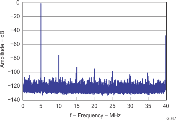 Figure 42. Spectrum With LF Noise Suppression Enabled (Fs = 80 MSPS)
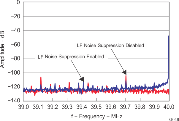 Figure 44. Zoomed Spectrum (39 to 40 MHz) With LF Noise Suppression Enabled (Fs = 80 MSPS)
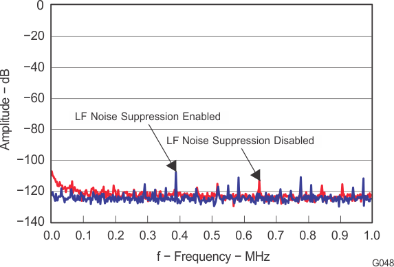 Figure 43. Zoomed Spectrum (DC to 1 MHz) With LF Noise Suppression Enabled (Fs = 80 MSPS)
7.3.2 Analog Input Circuit
The analog input consists of a switched-capacitor based differential sample and hold architecture as shown in Figure 45.
This differential topology results in good AC performance even for high input frequencies at high sampling rates. The INP and INM pins must be externally biased around a common-mode voltage of 1.5 V (VCM). For a full-scale differential input, each input pin (INP and INM) must swing symmetrically between VCM + 0.9 V and VCM – 0.9 V, resulting in a 3.6-VPP differential input swing.
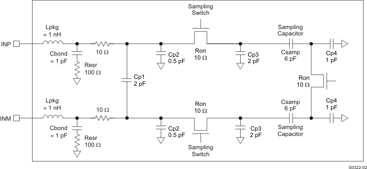 Figure 45. Input Stage
7.3.2.1 Drive Circuit Recommendations
For optimum performance, the analog inputs must be driven differentially which improves the common-mode noise immunity and even-order harmonic rejection. A resistor in series with each input pin (about 15 Ω) is recommended to damp out ringing caused by package parasitics. Low impedance (< 50 Ω) is required for the common-mode switching currents which can be achieved by using two resistors from each input terminated to the common-mode voltage (VCM).
The device includes an internal R-C filter from each input to ground. The purpose of this filter is to absorb the glitches caused by the opening and closing of the sampling capacitors. The filtering of the glitches can be improved further using an external R-C-R filter.
In addition to the previously listed requirements, the drive circuit may must be designed to provide a low insertion loss over the desired frequency range and matched impedance to the source. While doing this, the ADC input impedance must be considered. Figure 46 and Figure 47 show the impedance (Zin = Rin || Cin) looking into the ADC input pins.
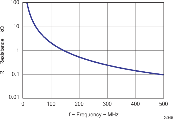 Figure 46. ADC Analog Input Resistance (Rin) Across Frequency
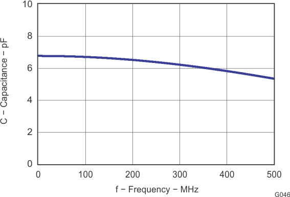 Figure 47. ADC Analog Input Capacitance (Cin) Across Frequency
7.3.2.2 Example Driving Circuit
Figure 48 shows an example input configuration using RF transformers. In this example, an external R-C-R filter using a 22-pF capacitor has been used. Together with the series inductor (39 nH), this combination forms a filter and absorbs the sampling glitches. Because of the relatively large capacitor (22 pF) in the R-C-R and the 15-Ω resistors in series with each input pin, this drive circuit has low bandwidth and is suited for low input frequencies.
The drive circuit has been terminated by 50 Ω near the ADC side. The termination is accomplished by a 25-Ω resistor from each input to the 1.5-V common-mode (VCM) from the device. This allows the analog inputs to be biased around the required common-mode voltage.
The mismatch in the transformer parasitic capacitance (between the windings) results in degraded even-order harmonic performance. Connecting two identical RF transformers back to back helps minimize this mismatch and good performance is obtained for high frequency input signals. An additional termination resistor pair may be required between the two transformers (enclosed by the dashed lines in Figure 48). The center point of this termination is connected to ground to improve the balance between the P and M sides. The values of the terminations between the transformers and on the secondary side must be chosen to get an effective 50 Ω (in the case of 50-Ω source impedance).
7.3.2.3 Input Common-Mode
To ensure a low-noise common-mode reference, the VCM pin is filtered with a 0.1-μF low-inductance capacitor connected to ground. The VCM pin is designed to directly drive the ADC inputs. Each input pin of the ADC sinks a common-mode current in the order of 6uA/MSPS(about 1mA at 80 MSPS) from the external drive circuit.
7.3.2.4 Programmable Fine Gain
ADS556x has programmable fine gain from 0 dB to 6dB in steps of 1 dB. The corresponding full-scale input range varies from 3.6 VPP down to 2 VPP. The fine gain is useful, when lower full-scale input ranges are used to get SFDR improvement (See Figure 11 and Figure 27). This is accompanied by corresponding degradation in SNR (see Figure 12 and Figure 28). The gain can be programmed using the register bits GAIN (Table 14).
After reset, the device is initialized to 1 dB fine gain when configured as Serial Interface Mode. The gain of the device in Parallel Mode will depend on the voltage applied on the SCLK pin. See Table 4 for details.
Table 1. Full-scale Input Range Across Gains (Serial Interface Mode)
| GAIN (dB) | CORRESPONDING FULL-SCALE INPUT RANGE (VPP) |
|---|---|
| 0 | 3.56 (1) |
| 1, default after reset | 3.56 |
| 2 | 3.2 |
| 3 | 2.85 |
| 4 | 2.55 |
| 5 | 2.27 |
| 6 | 2 |
7.4 Device Functional Modes
7.4.1 Low Sampling Frequency Operation
For best performance at high sampling frequencies, the ADS556x device uses a clock generator circuit to derive internal timing for the ADC. The clock generator operates from 80 MSPS down to 25 MSPS in the DEFAULT SPEED mode. The ADC enters this mode after applying reset (with serial interface configuration) or by tying SCLK pin to low (with parallel configuration).
For low sampling frequencies (below 25 MSPS), the ADC must be put in the LOW SPEED mode. This mode can be entered by one of the following:
7.4.2 Clock Input
The ADS556x clock input can be driven with either a differential clock signal or a single-ended clock input, with little or no difference in performance between both configurations. The common-mode voltage of the clock inputs is set to VCM using internal 5-kΩ resistors that connect the CLKP and CLKM pins to the VCM pin, as shown in Figure 49. This connection allows using transformer-coupled drive circuits for sine wave clock or AC-coupling for LVPECL, LVDS, and LVCMOS clock sources (Figure 50, Figure 51, Figure 52, and Figure 53).
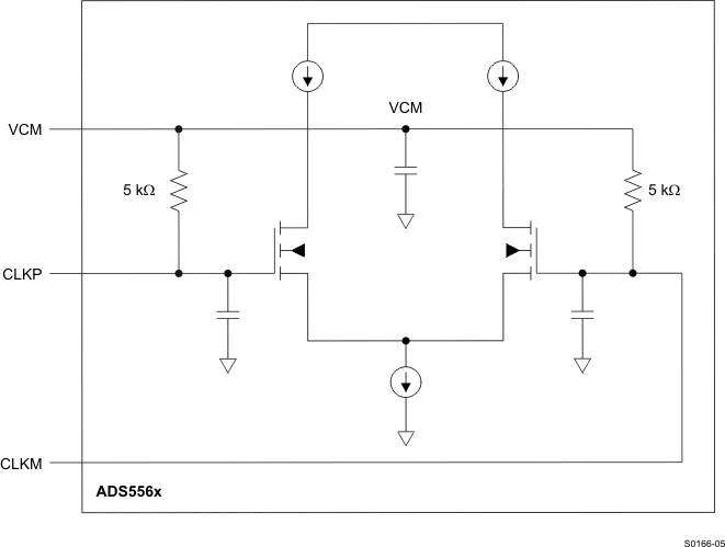 Figure 49. Clock Inputs
For best performance, the clock inputs must be driven differentially, reducing susceptibility to common-mode noise. For high input frequency sampling, TI recommends to use a clock source with very low jitter. Bandpass filtering of the clock source can help reduce the effect of jitter. No change in performance occurs with a non-50% duty cycle clock input. Single-ended CMOS clock can be AC-coupled to the CLKP input, with CLKM connected to ground with 0.1-µF capacitor, as shown in Figure 53.
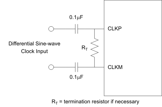 Figure 50. Differential Sine-Wave Clock Driving Circuit
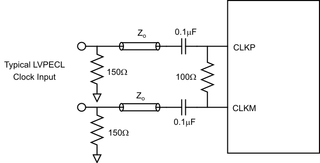 Figure 52. Typical LVPECL Clock Driving Circuit
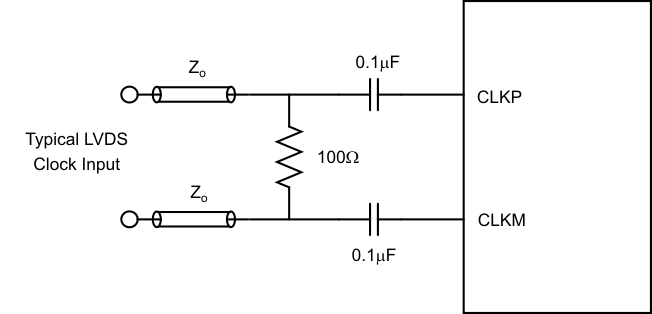 Figure 51. Typical LVDS Clock Driving Circuit
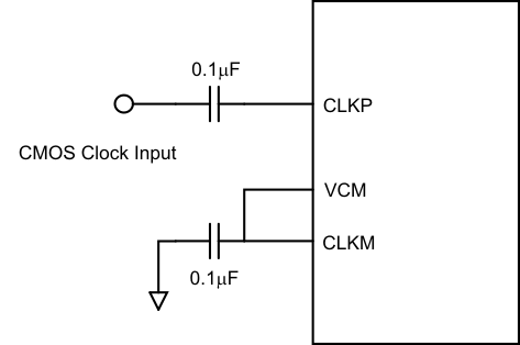 Figure 53. Typical LVCMOS Clock Driving Circuit
For high input frequency sampling, TI recommends using a clock source with very low jitter. Bandpass filtering of the clock source can help reduce the effect of jitter. A small change in performance occurs with a non-50% duty cycle clock input.
7.4.2.1 Power-Down
The ADS556x device has three power-down modes: global STANDBY, output buffer disabled, and input clock stopped.
7.4.2.1.1 Global STANDBY
This mode can be initiated by controlling SDATA or by setting the <STBY> register bit through the serial interface. In this mode, the ADC, reference block and the output buffers are powered down resulting in reduced total power dissipation of about 155 mW. The wake-up time from global power-down to valid data is typically 60 μs.
7.4.2.1.2 Output Buffer Disable
The output buffers can be disabled using the OE pin in both the LVDS and CMOS modes. With the buffers disabled, the digital outputs are in the tri-state. The wake-up time from this mode to data becoming valid in normal mode is typically 700 ns in LVDS mode and 200 ns in CMOS mode.
7.4.2.1.3 Input Clock Stop
The converter enters this mode when the input clock frequency falls below 1 MSPS. The power dissipation is about 125 mW and the wake-up time from this mode to data becoming valid in normal mode is typically 80 μs.
7.4.2.2 Power Supply Sequence
During power-up, the AVDD and DRVDD supplies can come up in any sequence. The two supplies are separated inside the device. Externally, the supplies can be driven from separate supplies or from a single supply.
7.4.3 Output Interface
The ADS556x device provides 16-bit data, an output clock synchronized with the data, and an out-of-range indicator that goes high when the output reaches the full-scale limits. In addition, output enable control (OE) is provided to power-down the output buffers and put the outputs in high-impedance state.
Two output interface options are available: Double Data Rate (DDR) LVDS and parallel CMOS. These options are selected using the DFS or the serial-interface <ODI> register bit (see Table 7).
7.4.3.1 DDR LVDS Outputs
In this mode, the 16 data bits and the output clock are put out using LVDS (low voltage differential signal) levels. Two successive data bits are multiplexed and output on each LVDS differential pair as shown in Figure 54. Therefore, 8 LVDS output pairs are available for the data bits and 1 LVDS output pair for the output clock.
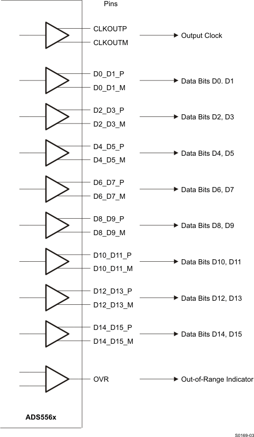 Figure 54. DDR LVDS Outputs
Even data bits (D0, D2 through D14) are output at the falling edge of CLKOUTP and the odd data bits (D1, D3 through D15) are output at the rising edge of CLKOUTP. Both the rising and falling edges of CLKOUTP must be used to capture all the data bits (see Figure 55).
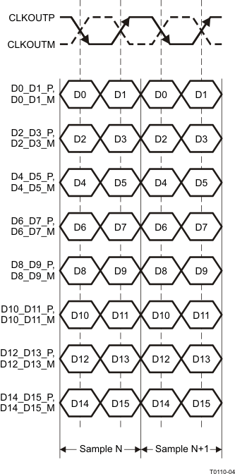 Figure 55. DDR LVDS Interface
7.4.3.2 LVDS Buffer Current Programmability
The default LVDS buffer output current is 3.5 mA. Terminating the buffer current by 100 Ω results in logic HIGH of 350 mV and logic LOW of –350 mV. The LVDS buffer currents can also be programmed to 2.5 mA, 4.5 mA, and 1.95 mA using the serial interface. In addition, exists a current double mode exists in which this current is doubled for the data and output clock buffers.
Both the buffer current programming and the current double mode can be done separately for the data buffers and the output clock buffer (<LVDS CURR> register bits).
7.4.3.3 LVDS Buffer Internal Termination
An internal termination option is available (using the serial interface), by which the LVDS buffers are differentially terminated inside the device. These termination resistances are available: 325, 200, and 175 Ω (nominal with ±20% variation). Any combination of these three terminations can be programmed; the effective termination will be the parallel combination of the selected resistances. This results in eight effective terminations from open (no termination) to 75 Ω.
The internal termination helps to absorb any reflections coming from the receiver end, improving the signal integrity. With 100-Ω internal and 100-Ω external termination, the voltage swing at the receiver end is halved (compared to no internal termination). The terminations can be controlled using the <DATA TERM> and <CLKOUT TERM> register bits.
The voltage swing can be restored by using the LVDS current double mode (<CURR DOUBLE> register bit).
7.4.3.4 Parallel CMOS
In this mode, the digital data and output clock are put out as 3.3-V CMOS voltage levels. Each data bit and the output clock is available on a separate pin in parallel. By default, the data outputs are valid during the rising edge of the output clock. The output clock is CLKOUT.
7.4.4 Output Data Format
Two output data formats are supported: 2s-complement and offset binary. These formats can be selected using the DFS pin or the serial-interface <DFS> register bit (see Table 9). In the event of an input voltage overdrive, the digital outputs go to the appropriate full scale level. For a positive overdrive, the output code is 0xFFFF in offset binary output format, and 0x7FFF in 2s-complement output format. For a negative input overdrive, the output code is 0x0000 in offset binary output format and 0x8000 in 2s complement output format.
7.4.5 Reference
The ADS556x device has a built-in internal reference that does not require external components. Design schemes are used to linearize the converter load seen by the reference; this and the integration of the requisite reference capacitors on-chip eliminates the need for external decoupling capacitors. The full-scale input range of the converter can be controlled in the external reference mode as explained in the External Reference section. The internal or external reference modes can be selected by controlling the MODE pin 23 (see Table 8 for details) or by programming the serial-interface <REF> register bit.
7.4.5.1 Internal Reference
When the device is in internal reference mode, the REFP and REFM voltages are generated internally. The common-mode voltage (1.5 V nominal) is output on VCM pin, which can be used to externally bias the analog input pins.
7.4.5.2 External Reference
When the device is in external reference mode, the VCM acts as a reference input pin. The voltage forced on the VCM pin is buffered and gained internally, generating the REFP and REFM voltages. The differential input voltage corresponding to full-scale is given by Equation 1. In this mode, the 1.5-V common-mode voltage to bias the input pins must be generated externally.
where
- G = 10–(Fine gain in db/20)
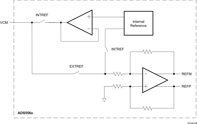 Figure 56. Reference Section
7.5 Programming
7.5.1 Device Programming Modes
The ADS556x device offers flexibility with several programmable features that are easily configured.
The device can be configured independently using either parallel interface control or serial interface programming.
In addition, the device supports a third configuration mode, where both the parallel interface and the serial control registers are used. In this mode, the priority between the parallel and serial interfaces is determined by a priority table (Table 3). If this additional level of flexibility is not required, the user can select either the serial interface programming or the parallel interface control.
7.5.2 Using Parallel Interface Control Only
To control the device using parallel interface, keep RESET tied to high (DRVDD). The DFS, MODE, SEN, SCLK, and SDATA pins are used to directly control certain modes of the ADC. The device is configured by connecting the parallel pins to the correct voltage levels (as described in Table 4 to Table 8). Applying a reset is not required.
In this mode, the SEN, SCLK, and SDATA pins function as parallel interface control pins. Frequently used functions are controlled in this mode: standby, selection between LVDS/CMOS output format, internal and external reference, 2s-complement and offset-binary output format, and position of the output clock edge.
Table 2 lists a description of the modes controlled by the parallel pins.
Table 2. Parallel Pin Definition
| PIN | CONTROL MODES |
|---|---|
| DFS | DATA FORMAT and the LVDS/CMOS output interface |
| MODE | Internal or external reference |
| SEN | CLKOUT edge programmability |
| SCLK | LOW SPEED mode control for low sampling frequencies (≤ 30 MSPS) |
| SDATA | STANDBY mode – Global (ADC, internal references and output buffers are powered down) |
7.5.2.1 Using Serial Interface Programming Only
To program using the serial interface, the internal registers must first be reset to the default values, and the RESET pin must be kept low. In this mode, the SEN, SDATA, and SCLK pins function as serial interface pins and are used to access the internal registers of ADC. The registers are reset either by applying a pulse on the RESET pin (of width greater than 10 ns), or by a high setting on the <RST> bit (D1 in register 0x6C). The Serial Interface section describes the register programming and register reset in more detail.
Because the parallel pins, DFS and MODE, are not used in this mode, they must be tied to ground.
7.5.2.2 Using Both Serial Interface And Parallel Controls
For increased flexibility, a combination of serial interface registers and parallel pin controls (DFS, MODE) can also be used to configure the device.
The serial registers must first be reset to the default values and the RESET pin must be kept low. In this mode, the SEN, SDATA, and SCLK pins function as serial interface pins and are used to access the internal registers of ADC. The registers are reset either by applying a pulse on RESET pin or by a high setting on the <RST> bit (D1 in register 0x6C). The Serial Interface section describes the register programming and register reset in more detail.
The parallel interface control pins, DFS and MODE, are used and their function is determined by the appropriate voltage levels as described in Table 7 and Table 8. The voltage levels are derived by using a resistor string as shown in Figure 57. Because some functions are controlled using both the parallel pins and serial registers, the priority between the two is determined by a priority table (Table 3).
Table 3. Priority Between Parallel Pins and Serial Registers
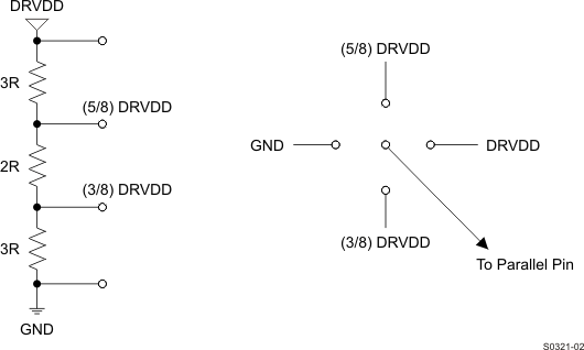 Figure 57. Simple Scheme to Configure Parallel Pins
7.5.2.3 Description of Parallel Pins
Table 4. SCLK Control Pin
| SCLK | DESCRIPTION |
|---|---|
| 0 | DEFAULT SPEED mode - Use for sampling frequencies > 25 MSPS, 3dB Gain. |
| DRVDD | LOW SPEED mode Enabled - Use for sampling frequencies ≤ 25 MSPS, 1dB Gain. |
Table 5. SDATA Control Pin
| SDATA | DESCRIPTION |
|---|---|
| 0 | Normal operation (Default) |
| DRVDD | STANDBY. This is a global power-down, where ADC, internal references and the output buffers are powered down. |
Table 6. SEN Control Pin
| SEN | DESCRIPTION |
|---|---|
| WITH CMOS INTERFACE | |
| 0 | CLKOUT Rising edge later by (3/36)Ts CLKOUT Falling edge later by (3/36)Ts |
| (3/8)DRVDD | CLKOUT Rising edge later by (5/36)Ts CLKOUT Falling edge later by (5/36)Ts |
| (5/8)DRVDD | CLKOUT Rising edge earlier by (3/36)Ts CLKOUT Falling edge earlier by (3/36)Ts |
| DRVDD | Default CLKOUT position |
| WITH LVDS INTERFACE | |
| 0 | CLKOUT Rising edge later by (7/36)Ts CLKOUT Falling edge later by (6/36)Ts |
| (3/8)DRVDD | CLKOUT Rising edge later by (7/36)Ts CLKOUT Falling edge later by (6/36)Ts |
| (5/8)DRVDD | CLKOUT Rising edge later by (3/36)Ts CLKOUT Falling edge later by (3/36)Ts |
| DRVDD | Default CLKOUT position |
Table 7. DFS Control Pin
| DFS | DESCRIPTION |
|---|---|
| 0 | 2s-complement data and DDR LVDS output (Default) |
| (3/8)DRVDD | 2s-complement data and parallel CMOS output |
| (5/8)DRVDD | Offset binary data and parallel CMOS output |
| DRVDD | Offset binary data and DDR LVDS output |
Table 8. MODE Control Pin
| MODE | DESCRIPTION |
|---|---|
| 0 | Internal reference |
| (3/8)AVDD | External reference |
| (5/8)AVDD | External reference |
| AVDD | Internal reference |
7.5.3 Serial Interface
The ADC has a set of internal registers, which can be accessed through the serial interface formed by the SEN (serial interface enable), SCLK (serial interface clock), SDATA (serial interface data), and RESET pins. After device power-up, the internal registers must be reset to the default values by applying a high-going pulse on RESET (of width greater than 10 ns), or by a high setting on the <RST> bit (D1 in register 0x6C).
A serial shift of bits into the device is enabled when the SEN pin is low. The serial data pin, SDATA, is latched at every falling edge of the SCLK pin when the SEN pin is active (low). The serial data is loaded into the register at every 16th SCLK falling edge when the SEN pin is low. If the word length exceeds a multiple of 16 bits, the excess bits are ignored. Data is loaded in multiples of 16-bit words within a single active SEN pulse.
The first 8 bits form the register address and the remaining 8 bits form the register data. The interface can work with a SCLK frequency from 20 MHz down to very low speeds (few Hertz) and also with non-50% SCLK duty cycle.
7.5.4 Register Initialization
After power-up, the internal registers must be reset to the default values which occurs in one of the following ways:
- A hardware reset by applying a high-going pulse on the RESET pin (of width greater than 10 ns) as shown in Figure 58.
- A software reset by using the serial interface and setting the <RST> bit (D1 in register 0x6C) to high. This configuration initializes the internal registers to the default values and then self-resets the <RST> bit to low. In this case the RESET pin is kept low.
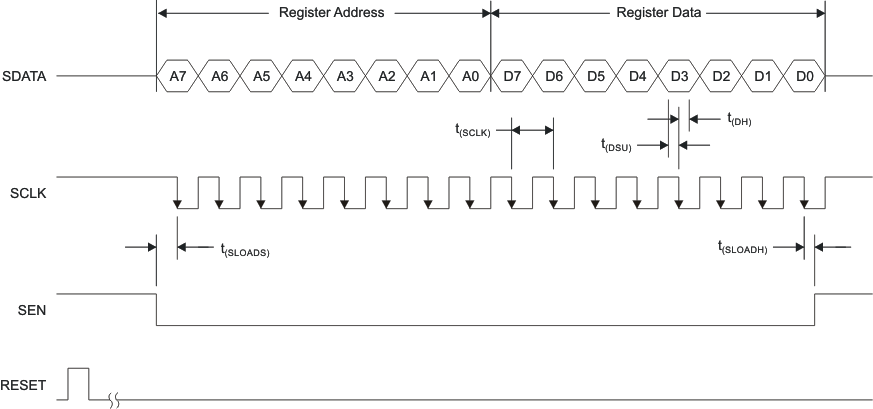 Figure 58. Serial Interface Timing Diagram
7.6 Register Maps
Table 9 gives a summary of all the modes that can be programmed through the serial interface.
Table 9. Summary of Functions Supported by Serial Interface(1) (2)
| REGISTER ADDRESS IN HEX |
REGISTER FUNCTIONS | |||||||
|---|---|---|---|---|---|---|---|---|
| A7 - A0 | D7 | D6 | D5 | D4 | D3 | D2 | D1 | D0 |
| 5D | <LF NOISE SUPPRESSION> | |||||||
| 62 | <CLKOUT POSN>
Output clock position programmability |
|||||||
| 63 | <STBY>
Global power down |
<DF>
DATA FORMAT - 2s complement or offset binary |
<LOW SPEED>
Enable low sampling frequency operation |
|||||
| 65 | <TEST PATTERN> – All 0s, all 1s, toggle, ramp, custom pattern | |||||||
| 68 | <GAIN>
Fine gain 0 dB to 6 dB, in 1-dB steps |
|||||||
| 69 | <CUSTOM A> Custom pattern (D7 TO D0) | |||||||
| 6A | <CUSTOM B> Custom pattern (D15 TO D8) | |||||||
| 6C | <ODI> Output data interface DDR LVDS or parallel CMOS |
|||||||
| 6D | <REF> Internal or external reference | |||||||
| 6E | <RST>
Software reset |
|||||||
| 7E | <DATA TERM>
Internal termination – data outputs |
<CLKOUT TERM>
Internal termination – output clock |
<LVDS CURR>
LVDS current programmability |
|||||
| 7F | <CURR DOUBLE>
LVDS current double |
|||||||
7.6.1 Register Description
This section explains each register function in detail.
Table 10. Register 5D
| A7 - A0 (hex) | D7 | D6 | D5 | D4 | D3 | D2 | D1 | D0 |
|---|---|---|---|---|---|---|---|---|
| 5D | <LF NOISE SUPPRESSION> |
| D0 | <LF NOISE SUPPRESSION> Low-Frequency Noise Suppression | |
| 0 | Disable low-frequency noise suppression | |
| 1 | Enable low-frequency noise suppression | |
Table 11. Register 62
| A7 - A0 (hex) | D7 | D6 | D5 | D4 | D3 | D2 | D1 | D0 |
|---|---|---|---|---|---|---|---|---|
| 62 | <CLKOUT POSN>
Output clock position programmability |
|||||||
| D4 - D0 | <CLKOUT POSN> Output Clock Position Programmability | |
| 00000 | Register value after reset (corresponds to default CLKOUT position) Setup/hold timings with this clock position are specified in the Timing Characteristics for LVDS and CMOS Modes table. |
|
| 00001 | Default CLKOUT position. Setup and hold timings with this clock position are specified in the Timing Characteristics for LVDS and CMOS Modes table. |
|
| XX011 | CMOS - Rising edge earlier by (3/36) Ts | |
| LVDS - Falling edge later by (3/36) Ts | ||
| XX101 | CMOS - Rising edge later by (3/36) Ts | |
| LVDS - Falling edge later by (6/36) Ts | ||
| XX111 | CMOS - Rising edge later by (5/36) Ts | |
| LVDS - Falling edge later by (6/36) Ts | ||
| 01XX1 | CMOS - Falling edge earlier by (3/36) Ts | |
| LVDS - Rising edge later by (3/36) Ts | ||
| 10XX1 | CMOS - Falling edge later by (3/36) Ts | |
| LVDS - Rising edge later by (7/36) Ts | ||
| 11XX1 | CMOS - Falling edge later by (5/36) Ts | |
| LVDS - Rising edge later by (7/36) Ts | ||
Table 12. Register 63
| A7 - A0 (hex) | D7 | D6 | D5 | D4 | D3 | D2 | D1 | D0 |
|---|---|---|---|---|---|---|---|---|
| 63 | <STBY>
Global power down |
<DF>
DATA FORMAT - 2s complement or offset binary |
<LOW SPEED>
Enable low sampling frequency operation |
| D3 | <DF> Output Data Format | |
| 0 | 2s-complement | |
| 1 | Offset binary | |
| D0 | <LOW SPEED> Low Sampling Frequency Operation | |
| 0 | DEFAULT SPEED mode (for Fs > 25 MSPS) | |
| 1 | LOW SPEED mode eabled (for Fs ≤ 25 MSPS) | |
| D7 | <STBY> Global STANDBY | |
| 0 | Normal operation | |
| 1 | Global power-down (includes ADC, internal references and output buffers) | |
Table 13. Register 65
| A7 - A0 (hex) | D7 | D6 | D5 | D4 | D3 | D2 | D1 | D0 |
|---|---|---|---|---|---|---|---|---|
| 65 | <TEST PATTERNS> — All 0s, all 1s, toggle, ramp, custom pattern | |||||||
| D7 - D5 | <TEST PATTERN> Outputs selected test pattern on data lines | |
| 000 | Normal operation | |
| 001 | All 0s | |
| 010 | All 1s | |
| 011 | Toggle pattern - alternate 1s and 0s on each data output and across data outputs | |
| 100 | Ramp pattern - Output data ramps from 0x0000 to 0xFFFF by one code every clock cycle | |
| 101 | Custom pattern - Outputs the custom pattern in CUSTOM PATTERN registers A and B | |
| 111 | Unused | |
Table 14. Register 68
| A7 - A0 (hex) | D7 | D6 | D5 | D4 | D3 | D2 | D1 | D0 |
|---|---|---|---|---|---|---|---|---|
| 68 | <GAIN> Fine gain 0 dB to 6 dB, in 1-dB steps | |||||||
| D3 - D0 | <GAIN> Programmable Fine Gain | |
| 0XXX | 1 dB | |
| 1000 | 0 dB | |
| 1001 | 1 dB, default register value after reset | |
| 1010 | 2 dB | |
| 1011 | 3 dB | |
| 1100 | 4 dB | |
| 1101 | 5 dB | |
| 1110 | 6 dB | |
Table 15. Register 69 and Register 6A
| A7 - A0 (hex) | D7 | D6 | D5 | D4 | D3 | D2 | D1 | D0 |
|---|---|---|---|---|---|---|---|---|
| 69 | <CUSTOM A> Custom pattern (D7–D0) | |||||||
| 6A | <CUSTOM B> Custom pattern (D15–D8) | |||||||
| Register 69 D7 - D0 |
<CUSTOM A> Custom pattern (D7–D0) | |
| Program bits D7 to D0 of custom pattern | ||
| Register 6A D15 - D8 |
<CUSTOM B> Custom pattern (D15–D8) | |
| Program bits D15 to D8 of custom pattern | ||
Table 16. Register 6C
| A7 - A0 (hex) | D7 | D6 | D5 | D4 | D3 | D2 | D1 | D0 |
|---|---|---|---|---|---|---|---|---|
| 6C | <ODI> Output data interface - DDR LVDS or parallel CMOS | |||||||
| D4 - D3 | <ODI> Output Interface | |
| 00 | default after reset, state of DFS pin determines interface type. See Table 7. | |
| 01 | DDR LVDS outputs, independent of state of DFS pin. | |
| 11 | Parallel CMOS outputs, independent of state of DFS pin. | |
Table 17. Register 6D
| A7 - A0 | D7 | D6 | D5 | D4 | D3 | D2 | D1 | D0 |
|---|---|---|---|---|---|---|---|---|
| 6D | <REF>
Internal or external reference |
| D4 | <REF> Reference | |
| 0 | Internal reference | |
| 1 | External reference mode, force voltage on VCM to set reference. | |
Table 18. Register 6E
| A7 - A0 | D7 | D6 | D5 | D4 | D3 | D2 | D1 | D0 |
|---|---|---|---|---|---|---|---|---|
| 6E | <RST> Software reset |
| D0 | <RST> Software resets the ADC | |
| 1 | Resets all registers to default values | |
Table 19. Register 7E
| A7 - A0 | D7 | D6 | D5 | D4 | D3 | D2 | D1 | D0 |
|---|---|---|---|---|---|---|---|---|
| 7E | <DATA TERM> Internal termination – data outputs | <CLKOUT TERM> Internal termination – output clock | <LVDS CURR> LVDS current programmability | |||||
| D1 - D0 | <LVDS CURR> LVDS Buffer Current Programmability | |
| 00 | 3.5 mA, default | |
| 01 | 2.5 mA | |
| 10 | 4.5 mA | |
| 11 | 1.75 mA | |
| D4 - D2 | <CLKOUT TERM> LVDS Buffer Internal Termination | |
| 000 | No internal termination | |
| 001 | 325 | |
| 010 | 200 | |
| 011 | 125 | |
| 100 | 170 | |
| 101 | 120 | |
| 110 | 100 | |
| 111 | 75 | |
| D7 - D5 | <DATA TERM> LVDS Buffer Internal Termination | |
| 000 | No internal termination | |
| 001 | 325 | |
| 010 | 200 | |
| 011 | 125 | |
| 100 | 170 | |
| 101 | 120 | |
| 110 | 100 | |
| 111 | 75 | |
Table 20. Register 7F
| A7 - A0 | D7 | D6 | D5 | D4 | D3 | D2 | D1 | D0 |
|---|---|---|---|---|---|---|---|---|
| 7F | <CURR DOUBLE> LVDS current double | |||||||
| D7 - D6 | <CURR DOUBLE> LVDS Buffer Internal Termination | |
| 00 | Value specified by <LVDS CURR> | |
| 01 | 2x data, 2x clockout currents | |
| 10 | 1x data, 2x clockout currents | |
| 11 | 2x data, 4x clockout currents | |
8 Application and Implementation
NOTE
Information in the following applications sections is not part of the TI component specification, and TI does not warrant its accuracy or completeness. TI’s customers are responsible for determining suitability of components for their purposes. Customers should validate and test their design implementation to confirm system functionality.
8.1 Application Information
In the design of any application involving a high-speed data converter, particular attention should be paid to the design of the analog input, the clocking solution, and careful layout of the clock and analog signals. The ADS5562 evaluation module (EVM) is one practical example of the design of the analog input circuit and clocking solution, as well as a practical example of good circuit board layout practices around the ADC.
8.2 Typical Application
The analog inputs of the ADS5562 device must be fully differential and biased to an appropriate common mode voltage, VCM. End equipment typically does not have a signal that already meets the requisite amplitude and common mode and is fully differential. Therefore, a signal conditioning circuit is required for the analog input. If the amplitude of the input circuit is such that no gain is needed to make full use of the full-scale range of the ADC, then a transformer coupled circuit as used on the EVM can be used with good results. The transformer coupling is inherently low-noise, and inherently AC-coupled so that the signal may be biased to VCM after the transformer coupling. Figure 59 shows an example of transformer coupling as used on the ADS556x EVM.
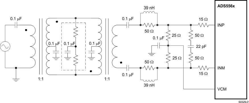 Figure 59. Drive Circuit Using RF Transformers
If signal gain is required, or the input bandwidth is to include the spectrum all the way down to DC such that AC coupling is not possible, then an amplifier-based signal conditioning circuit would be required. Figure 60 shows the LMH6552 device interfaced with the ADS5562 device. The LMH6552 device is configured to have to single-ended input with a differential outputs follow by the first Nyquist-based low-pass filter with 40-MHz bandwidth. Figure 60 also shows the power supply recommendations for the amplifier.
 Figure 60. Drive Circuit Using LMH6552 Fully Differential Amplifier
Clocking a high-speed ADC such as the ADS5562 device requires a fully differential-clock signal from a clean, low-jitter clock source and driven by an appropriate clock buffer, often with LVPECL or LVDS signaling levels. The sample clock must also be biased up to the appropriate common mode voltage, but unlike the analog input, the data converter itself will often internally bias the clock to the appropriate VCM if the clock signal is AC coupled as in the typical clock driver circuit shown in Figure 50 through Figure 53.
8.2.1 Design Requirements
The ADS5562 device requires a fully differential analog input with a full-scale range not to exceed 3.56-V peak-to-peak differential, biased to a common-mode voltage of 1.5 V. In addition the input circuit must provide proper transmission line termination (or proper load resistors in an amplifier-based solution) so the input of the impedance of the ADC analog inputs should be considered as well.
The ADS5562 device is capable of a typical SNR of 82.8 dBFS for input frequencies of about 30 MHz, which is well under the Nyquist limit for this ADC operating at 80 Msps. The amplifier and clocking solution have a direct impact on performance in terms of SNR. Therefore the amplifier and clocking solution should be selected such that the SNR performance of at least 82 dBFS is preserved.
8.2.2 Detailed Design Procedure
The ADS5562 device has a maximum sample rate of 80 MHz and an input bandwidth of approximately 300 MHz. For this application, the first Nyquist zone is involved, so the frequency bandwidth must be limited under 40 MHz.
8.2.2.1 Clocking Source for ADC5562
The signal-to-noise ratio of the ADC is limited by three different factors: the quantization noise, the thermal noise, and the total jitter of the sample clock. Quantization noise is driven by the resolution of the ADC, which is 16 bits for the ADS5562 device. Thermal noise is typically not noticeable in high-speed pipelined converters such as the ADS5562 device, but may be estimated by looking at the signal to noise ratio of the ADC with very-low input frequencies and using Equation 3 to solve for thermal noise. For this estimation, use the specified SNR for the lowest frequency listed (see the Specifications section. The lowest input frequency listed for the ADS5562 device is at 3 MHz, and the SNR at that frequency is 84 dB. Therefore, use 84 dB as the SNR limit for this application because of thermal noise. This value is just an approximation, and the lower the input frequency that has an SNR specification the better this approximation is. The thermal noise limits the SNR at low input frequencies while the clock jitter sets the SNR for higher input frequencies.
Quantization noise is also a limiting factor for SNR, as the theoretical maximum achievable SNR as a function of the number of bits of resolution is set by Equation 2.

where
- N = number of bits resolution.
For a 16-bit ADC, the maximum SNR = 1.76 + (6.02 × 16) = 98.08 dB. This value is the number that is entered into Equation 3 for quantization noise as we solve for total SNR for different amounts of clock jitter using Equation 3.

Use Equation 4 to calculate the SNR limitation because of sample clock jitter.

Note that the clock jitter in Equation 4 is the total amount of clock jitter, whether the jitter source is internal to the ADC or external because of the clocking source. The total clock jitter (TJitter) has two components – the internal aperture jitter (90 fs for ADS5562) which is set by the noise of the clock input buffer, and the external clock jitter from the clocking source and all associated buffering of the clock signal. Use Equation 5 to calculate the total clock jitter from the aperture jitter and the external clock jitter.

The external clock jitter can be minimized by using high-quality clock sources and jitter cleaners as well as a bandpass filter at the clock input while a faster clock slew rate may at times also improve the ADC aperture jitter slightly.
The ADS5562 device has an internal aperture jitter of 90 fs, which is largely fixed. The SNR depending on amount of external jitter for different input frequencies is shown in Figure 61. Often the design requirements list a target SNR for a system, and Equation 3 through Equation 5 are then used to calculate the external clock jitter needed from the clocking solution to meet the system objectives.
Figure 61 shows that with an external clock jitter of 200 fs rms, the expected SNR of the ADS5562 device is greater than 82 dBFS at an input tone of 40 MHz, which is the Nyquist limit. Having less external clock jitter such as 150 fs rms, or even 100 fs rms, results in an SNR that exceeds the design target, but possibly at the expense of a more costly clocking solution. An external clock jitter of greater than 200 fs does not meet the design target. Because the design target for SNR is established at 82 dB, and a margin of error is necessary for the SNR contribution from the amplifier and filter on the analog signal, the design goal of 150 fs external clock jitter is established to achieve an SNR for the ADC of approximately 83 dB.
8.2.2.2 Amplifier Selection
The amplifier and any input filtering has its own SNR performance, and the SNR performance of the amplifier front end combines with the SNR of the ADC to yield a system SNR that is less than that of the ADC. System SNR can be calculated from the SNR of the amplifier conditioning circuit and the overall ADC SNR as in Equation 6. In Equation 6, the SNR of the ADC is the value derived from the data sheet specifications and the clocking derivation presented in the Clocking Source for ADC5562 section.

The SNR of the amplifier and filter can be calculated from the noise specifications in the data sheet for the amplifier, the amplitude of the signal and the bandwidth of the filter. The noise from the amplifier is band-limited by the filter, and the rolloff of the filter depends on the order of the filter. Therefore, replacing the filter rolloff with an equivalent brick-wall filter bandwidth is convenient. For example, a 1st order filter can be approximated by a brick-wall filter with bandwidth of 1.57 times the bandwidth of the 1st order filter. For this design, assume a 1st order filter is used. Use Equation 7 to calculate the amplifier and filter noise.

where
- VO = the amplifier output signal (which will be full scale input of the ADC expressed in rms)
- EFILTEROUT = ENAMPOUT × √ENB
- ENAMPOUT = the output noise density of the LMH6552 (1.1 nV/√Hz times amplifier gain)
- ENB = the brick-wall equivalent noise bandwidth of the filter
In Equation 7, the parameters of the equation may be seen to be in terms of signal amplitude in the numerator and amplifier noise in the denominator, or SNR. For the numerator, use the full-scale voltage specification of the ADS5562 device, or 3.56-V peak-to-peak differential. Because Equation 7 requires the signal voltage to be in rms, convert 3.56 VPP to 1.26 V rms.
The noise specification for the LMH6552 device is listed as 1.1 nV/√Hz times the amplifier gain. Therefore, use this value to integrate the noise component from DC out to the filter cutoff, using the equivalent brick wall filter of 40 MHz × 1.57, or 62.8 MHz. The result of 1.1 nV/√Hz over √62.8 MHz times gain yields 8717 nV, or 8.717 µV, assuming a gain factor of 2 for the amplifier.
Using 1.26-V rms for VO and 8.717 µV for EFILTEROUT, the SNR of the amplifier and filter as given by Equation 7 is approximately 103.2 dB.
Taking the SNR of the ADC as 83 dB from Figure 61, and SNR of the amplifier and filter as 103.2 dB, Equation 6 predicts the system SNR to be 82.96 dB. In other words, the SNR of the ADC and the SNR of the front end combine as the square root of the sum of squares, and because the SNR of the amplifier front end is much greater than the SNR of the ADC in this example, the SNR of the ADC dominates Equation 6 and the system SNR is almost the SNR of the ADC. The assumed design requirement is 82 dB, and after a clocking solution was selected and an amplifier or filter solution was selected, the predicted SNR of is 82.96 dB. At this point, consider making tradeoffs of either the clocking specification or amplifier gain to see how such tradeoffs begin to affect the expected system performance.
8.2.3 Application Curve
Figure 61 shows the SNR of the ADC as a function of clock jitter and input frequency for the ADS5562 device. This plot of curves take into account the aperture jitter of the ADC, the number of bits of resolution, and the thermal noise estimation so that the plot can be used to predict SNR for a given input frequency and external clock jitter. Figure 61 then may be used to set the jitter requirement for the clocking solution for a given input bandwidth and given design goal for SNR.
 Figure 61. SNR vs Input Frequency and External Clock Jitter
