SLWS207B May 2008 – January 2016 ADS5560 , ADS5562
PRODUCTION DATA.
- 1 Features
- 2 Applications
- 3 Description
- 4 Revision History
- 5 Pin Configuration and Functions
-
6 Specifications
- 6.1 Absolute Maximum Ratings
- 6.2 ESD Ratings
- 6.3 Recommended Operating Conditions
- 6.4 Thermal Information
- 6.5 Electrical Characteristics
- 6.6 AC Electrical Characteristics for ADS5560 Fs = 40 MSPS
- 6.7 AC Electrical Characteristics for ADS5562, Fs = 80 MSPS
- 6.8 Electrical Characteristics for ADS5562
- 6.9 Electrical Characteristics for ADS5560
- 6.10 Digital Characteristics
- 6.11 Timing Characteristics for LVDS and CMOS Modes
- 6.12 Serial Interface Timing Characteristics
- 6.13 Reset Timing
- 6.14 Timing Characteristics at Lower Sampling Frequencies
- 6.15 Typical Characteristics
- 7 Detailed Description
- 8 Application and Implementation
- 9 Power Supply Recommendations
- 10Layout
- 11Device and Documentation Support
- 12Mechanical, Packaging, and Orderable Information
パッケージ・オプション
メカニカル・データ(パッケージ|ピン)
- RGZ|48
サーマルパッド・メカニカル・データ
- RGZ|48
発注情報
7 Detailed Description
7.1 Overview
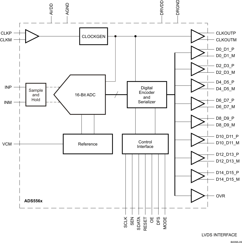
The ADS556x device is a high-performance 16-bit ADC family with sampling rates up to 80 MSPS. The device is based on switched capacitor technology and runs off a single 3.3-V supply. When the signal is captured by the input sample and hold, the input sample is sequentially converted by a series of small resolution stages. At every clock edge, the sample propagates through the pipeline resulting in a data latency of 16 clock cycles. The output is available as 16-bit data, in DDR LVDS or parallel CMOS and coded in either offset binary or binary 2s-complement format.
7.2 Functional Block Diagram
7.3 Feature Description
7.3.1 Low-Frequency Noise Suppression
The low-frequency noise suppression mode is specifically useful in applications where good noise performance is desired in the low-frequency band of DC to 1 MHz. Setting this mode shifts the low-frequency noise of the ADS556x device to approximately (Fs / 2), thereby moving the noise floor around DC to a much lower value. The <LF NOISE SUPPRESSION> register bit enables this mode. As Figure 43 shows, when the mode is enabled, the noise floor from DC to 1 MHz improves significantly. The low-frequency noise components get shifted to the region around Fs / 2 (Figure 44).
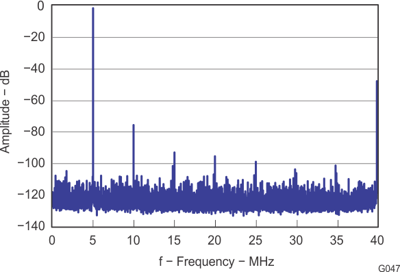 Figure 42. Spectrum With LF Noise Suppression Enabled (Fs = 80 MSPS)
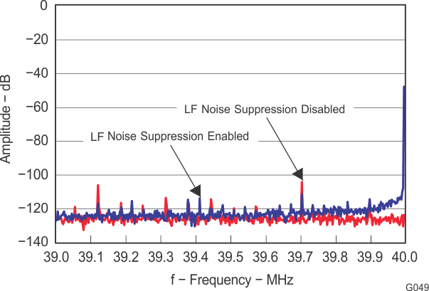 Figure 44. Zoomed Spectrum (39 to 40 MHz) With LF Noise Suppression Enabled (Fs = 80 MSPS)
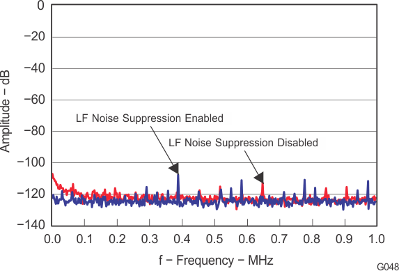 Figure 43. Zoomed Spectrum (DC to 1 MHz) With LF Noise Suppression Enabled (Fs = 80 MSPS)
7.3.2 Analog Input Circuit
The analog input consists of a switched-capacitor based differential sample and hold architecture as shown in Figure 45.
This differential topology results in good AC performance even for high input frequencies at high sampling rates. The INP and INM pins must be externally biased around a common-mode voltage of 1.5 V (VCM). For a full-scale differential input, each input pin (INP and INM) must swing symmetrically between VCM + 0.9 V and VCM – 0.9 V, resulting in a 3.6-VPP differential input swing.
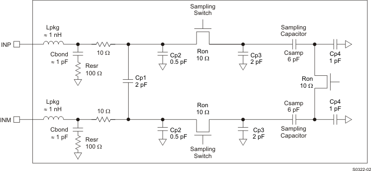 Figure 45. Input Stage
7.3.2.1 Drive Circuit Recommendations
For optimum performance, the analog inputs must be driven differentially which improves the common-mode noise immunity and even-order harmonic rejection. A resistor in series with each input pin (about 15 Ω) is recommended to damp out ringing caused by package parasitics. Low impedance (< 50 Ω) is required for the common-mode switching currents which can be achieved by using two resistors from each input terminated to the common-mode voltage (VCM).
The device includes an internal R-C filter from each input to ground. The purpose of this filter is to absorb the glitches caused by the opening and closing of the sampling capacitors. The filtering of the glitches can be improved further using an external R-C-R filter.
In addition to the previously listed requirements, the drive circuit may must be designed to provide a low insertion loss over the desired frequency range and matched impedance to the source. While doing this, the ADC input impedance must be considered. Figure 46 and Figure 47 show the impedance (Zin = Rin || Cin) looking into the ADC input pins.
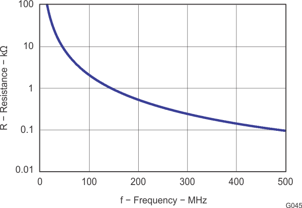 Figure 46. ADC Analog Input Resistance (Rin) Across Frequency
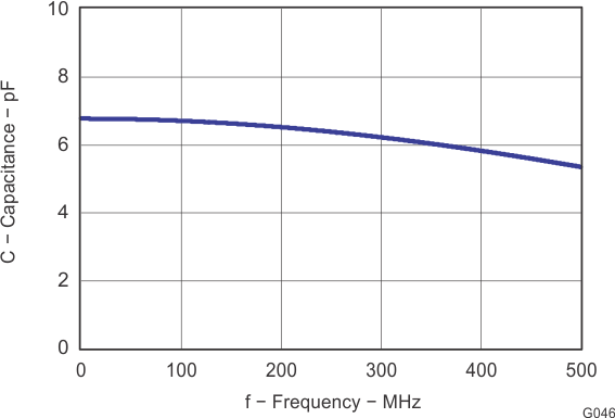 Figure 47. ADC Analog Input Capacitance (Cin) Across Frequency
7.3.2.2 Example Driving Circuit
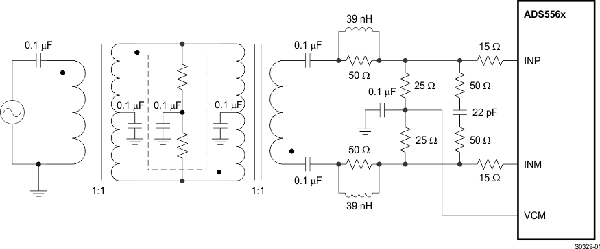
Figure 48 shows an example input configuration using RF transformers. In this example, an external R-C-R filter using a 22-pF capacitor has been used. Together with the series inductor (39 nH), this combination forms a filter and absorbs the sampling glitches. Because of the relatively large capacitor (22 pF) in the R-C-R and the 15-Ω resistors in series with each input pin, this drive circuit has low bandwidth and is suited for low input frequencies.
The drive circuit has been terminated by 50 Ω near the ADC side. The termination is accomplished by a 25-Ω resistor from each input to the 1.5-V common-mode (VCM) from the device. This allows the analog inputs to be biased around the required common-mode voltage.
The mismatch in the transformer parasitic capacitance (between the windings) results in degraded even-order harmonic performance. Connecting two identical RF transformers back to back helps minimize this mismatch and good performance is obtained for high frequency input signals. An additional termination resistor pair may be required between the two transformers (enclosed by the dashed lines in Figure 48). The center point of this termination is connected to ground to improve the balance between the P and M sides. The values of the terminations between the transformers and on the secondary side must be chosen to get an effective 50 Ω (in the case of 50-Ω source impedance).
7.3.2.3 Input Common-Mode
To ensure a low-noise common-mode reference, the VCM pin is filtered with a 0.1-μF low-inductance capacitor connected to ground. The VCM pin is designed to directly drive the ADC inputs. Each input pin of the ADC sinks a common-mode current in the order of 6uA/MSPS(about 1mA at 80 MSPS) from the external drive circuit.
7.3.2.4 Programmable Fine Gain
ADS556x has programmable fine gain from 0 dB to 6dB in steps of 1 dB. The corresponding full-scale input range varies from 3.6 VPP down to 2 VPP. The fine gain is useful, when lower full-scale input ranges are used to get SFDR improvement (See Figure 11 and Figure 27). This is accompanied by corresponding degradation in SNR (see Figure 12 and Figure 28). The gain can be programmed using the register bits GAIN (Table 14).
After reset, the device is initialized to 1 dB fine gain when configured as Serial Interface Mode. The gain of the device in Parallel Mode will depend on the voltage applied on the SCLK pin. See Table 4 for details.
Table 1. Full-scale Input Range Across Gains (Serial Interface Mode)
| GAIN (dB) | CORRESPONDING FULL-SCALE INPUT RANGE (VPP) |
|---|---|
| 0 | 3.56 (1) |
| 1, default after reset | 3.56 |
| 2 | 3.2 |
| 3 | 2.85 |
| 4 | 2.55 |
| 5 | 2.27 |
| 6 | 2 |
7.4 Device Functional Modes
7.4.1 Low Sampling Frequency Operation
For best performance at high sampling frequencies, the ADS556x device uses a clock generator circuit to derive internal timing for the ADC. The clock generator operates from 80 MSPS down to 25 MSPS in the DEFAULT SPEED mode. The ADC enters this mode after applying reset (with serial interface configuration) or by tying SCLK pin to low (with parallel configuration).
For low sampling frequencies (below 25 MSPS), the ADC must be put in the LOW SPEED mode. This mode can be entered by one of the following:
7.4.2 Clock Input
The ADS556x clock input can be driven with either a differential clock signal or a single-ended clock input, with little or no difference in performance between both configurations. The common-mode voltage of the clock inputs is set to VCM using internal 5-kΩ resistors that connect the CLKP and CLKM pins to the VCM pin, as shown in Figure 49. This connection allows using transformer-coupled drive circuits for sine wave clock or AC-coupling for LVPECL, LVDS, and LVCMOS clock sources (Figure 50, Figure 51, Figure 52, and Figure 53).
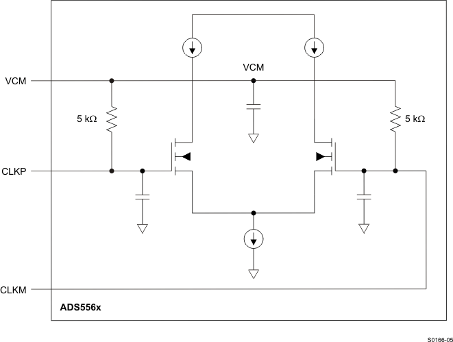 Figure 49. Clock Inputs
For best performance, the clock inputs must be driven differentially, reducing susceptibility to common-mode noise. For high input frequency sampling, TI recommends to use a clock source with very low jitter. Bandpass filtering of the clock source can help reduce the effect of jitter. No change in performance occurs with a non-50% duty cycle clock input. Single-ended CMOS clock can be AC-coupled to the CLKP input, with CLKM connected to ground with 0.1-µF capacitor, as shown in Figure 53.
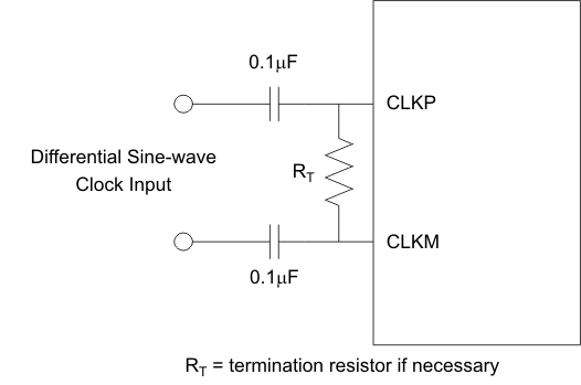 Figure 50. Differential Sine-Wave Clock Driving Circuit
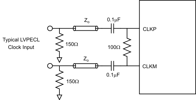 Figure 52. Typical LVPECL Clock Driving Circuit
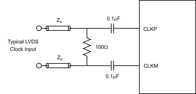 Figure 51. Typical LVDS Clock Driving Circuit
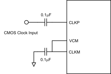 Figure 53. Typical LVCMOS Clock Driving Circuit
For high input frequency sampling, TI recommends using a clock source with very low jitter. Bandpass filtering of the clock source can help reduce the effect of jitter. A small change in performance occurs with a non-50% duty cycle clock input.
7.4.2.1 Power-Down
The ADS556x device has three power-down modes: global STANDBY, output buffer disabled, and input clock stopped.
7.4.2.1.1 Global STANDBY
This mode can be initiated by controlling SDATA or by setting the <STBY> register bit through the serial interface. In this mode, the ADC, reference block and the output buffers are powered down resulting in reduced total power dissipation of about 155 mW. The wake-up time from global power-down to valid data is typically 60 μs.
7.4.2.1.2 Output Buffer Disable
The output buffers can be disabled using the OE pin in both the LVDS and CMOS modes. With the buffers disabled, the digital outputs are in the tri-state. The wake-up time from this mode to data becoming valid in normal mode is typically 700 ns in LVDS mode and 200 ns in CMOS mode.
7.4.2.1.3 Input Clock Stop
The converter enters this mode when the input clock frequency falls below 1 MSPS. The power dissipation is about 125 mW and the wake-up time from this mode to data becoming valid in normal mode is typically 80 μs.
7.4.2.2 Power Supply Sequence
During power-up, the AVDD and DRVDD supplies can come up in any sequence. The two supplies are separated inside the device. Externally, the supplies can be driven from separate supplies or from a single supply.
7.4.3 Output Interface
The ADS556x device provides 16-bit data, an output clock synchronized with the data, and an out-of-range indicator that goes high when the output reaches the full-scale limits. In addition, output enable control (OE) is provided to power-down the output buffers and put the outputs in high-impedance state.
Two output interface options are available: Double Data Rate (DDR) LVDS and parallel CMOS. These options are selected using the DFS or the serial-interface <ODI> register bit (see Table 7).
7.4.3.1 DDR LVDS Outputs
In this mode, the 16 data bits and the output clock are put out using LVDS (low voltage differential signal) levels. Two successive data bits are multiplexed and output on each LVDS differential pair as shown in Figure 54. Therefore, 8 LVDS output pairs are available for the data bits and 1 LVDS output pair for the output clock.
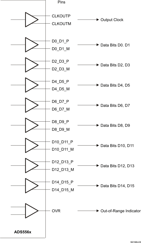 Figure 54. DDR LVDS Outputs
Even data bits (D0, D2 through D14) are output at the falling edge of CLKOUTP and the odd data bits (D1, D3 through D15) are output at the rising edge of CLKOUTP. Both the rising and falling edges of CLKOUTP must be used to capture all the data bits (see Figure 55).
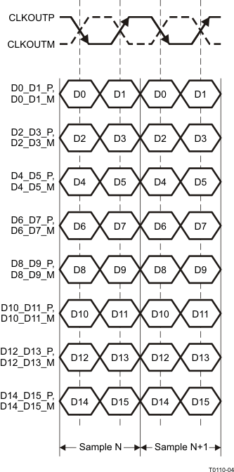 Figure 55. DDR LVDS Interface
7.4.3.2 LVDS Buffer Current Programmability
The default LVDS buffer output current is 3.5 mA. Terminating the buffer current by 100 Ω results in logic HIGH of 350 mV and logic LOW of –350 mV. The LVDS buffer currents can also be programmed to 2.5 mA, 4.5 mA, and 1.95 mA using the serial interface. In addition, exists a current double mode exists in which this current is doubled for the data and output clock buffers.
Both the buffer current programming and the current double mode can be done separately for the data buffers and the output clock buffer (<LVDS CURR> register bits).
7.4.3.3 LVDS Buffer Internal Termination
An internal termination option is available (using the serial interface), by which the LVDS buffers are differentially terminated inside the device. These termination resistances are available: 325, 200, and 175 Ω (nominal with ±20% variation). Any combination of these three terminations can be programmed; the effective termination will be the parallel combination of the selected resistances. This results in eight effective terminations from open (no termination) to 75 Ω.
The internal termination helps to absorb any reflections coming from the receiver end, improving the signal integrity. With 100-Ω internal and 100-Ω external termination, the voltage swing at the receiver end is halved (compared to no internal termination). The terminations can be controlled using the <DATA TERM> and <CLKOUT TERM> register bits.
The voltage swing can be restored by using the LVDS current double mode (<CURR DOUBLE> register bit).
7.4.3.4 Parallel CMOS
In this mode, the digital data and output clock are put out as 3.3-V CMOS voltage levels. Each data bit and the output clock is available on a separate pin in parallel. By default, the data outputs are valid during the rising edge of the output clock. The output clock is CLKOUT.
7.4.4 Output Data Format
Two output data formats are supported: 2s-complement and offset binary. These formats can be selected using the DFS pin or the serial-interface <DFS> register bit (see Table 9). In the event of an input voltage overdrive, the digital outputs go to the appropriate full scale level. For a positive overdrive, the output code is 0xFFFF in offset binary output format, and 0x7FFF in 2s-complement output format. For a negative input overdrive, the output code is 0x0000 in offset binary output format and 0x8000 in 2s complement output format.
7.4.5 Reference
The ADS556x device has a built-in internal reference that does not require external components. Design schemes are used to linearize the converter load seen by the reference; this and the integration of the requisite reference capacitors on-chip eliminates the need for external decoupling capacitors. The full-scale input range of the converter can be controlled in the external reference mode as explained in the External Reference section. The internal or external reference modes can be selected by controlling the MODE pin 23 (see Table 8 for details) or by programming the serial-interface <REF> register bit.
7.4.5.1 Internal Reference
When the device is in internal reference mode, the REFP and REFM voltages are generated internally. The common-mode voltage (1.5 V nominal) is output on VCM pin, which can be used to externally bias the analog input pins.
7.4.5.2 External Reference
When the device is in external reference mode, the VCM acts as a reference input pin. The voltage forced on the VCM pin is buffered and gained internally, generating the REFP and REFM voltages. The differential input voltage corresponding to full-scale is given by Equation 1. In this mode, the 1.5-V common-mode voltage to bias the input pins must be generated externally.
where
- G = 10–(Fine gain in db/20)
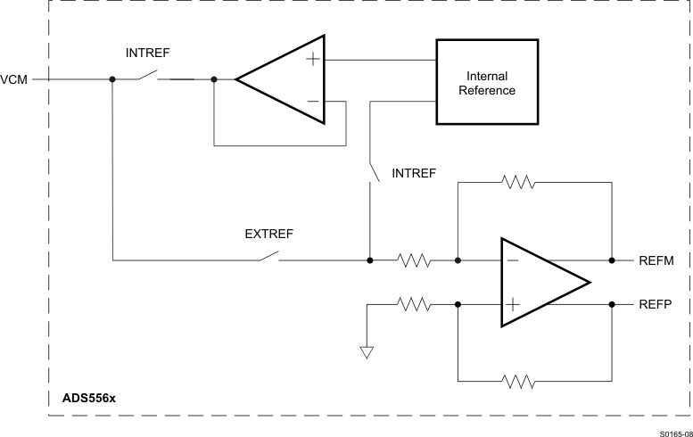 Figure 56. Reference Section
7.5 Programming
7.5.1 Device Programming Modes
The ADS556x device offers flexibility with several programmable features that are easily configured.
The device can be configured independently using either parallel interface control or serial interface programming.
In addition, the device supports a third configuration mode, where both the parallel interface and the serial control registers are used. In this mode, the priority between the parallel and serial interfaces is determined by a priority table (Table 3). If this additional level of flexibility is not required, the user can select either the serial interface programming or the parallel interface control.
7.5.2 Using Parallel Interface Control Only
To control the device using parallel interface, keep RESET tied to high (DRVDD). The DFS, MODE, SEN, SCLK, and SDATA pins are used to directly control certain modes of the ADC. The device is configured by connecting the parallel pins to the correct voltage levels (as described in Table 4 to Table 8). Applying a reset is not required.
In this mode, the SEN, SCLK, and SDATA pins function as parallel interface control pins. Frequently used functions are controlled in this mode: standby, selection between LVDS/CMOS output format, internal and external reference, 2s-complement and offset-binary output format, and position of the output clock edge.
Table 2 lists a description of the modes controlled by the parallel pins.
Table 2. Parallel Pin Definition
| PIN | CONTROL MODES |
|---|---|
| DFS | DATA FORMAT and the LVDS/CMOS output interface |
| MODE | Internal or external reference |
| SEN | CLKOUT edge programmability |
| SCLK | LOW SPEED mode control for low sampling frequencies (≤ 30 MSPS) |
| SDATA | STANDBY mode – Global (ADC, internal references and output buffers are powered down) |
7.5.2.1 Using Serial Interface Programming Only
To program using the serial interface, the internal registers must first be reset to the default values, and the RESET pin must be kept low. In this mode, the SEN, SDATA, and SCLK pins function as serial interface pins and are used to access the internal registers of ADC. The registers are reset either by applying a pulse on the RESET pin (of width greater than 10 ns), or by a high setting on the <RST> bit (D1 in register 0x6C). The Serial Interface section describes the register programming and register reset in more detail.
Because the parallel pins, DFS and MODE, are not used in this mode, they must be tied to ground.
7.5.2.2 Using Both Serial Interface And Parallel Controls
For increased flexibility, a combination of serial interface registers and parallel pin controls (DFS, MODE) can also be used to configure the device.
The serial registers must first be reset to the default values and the RESET pin must be kept low. In this mode, the SEN, SDATA, and SCLK pins function as serial interface pins and are used to access the internal registers of ADC. The registers are reset either by applying a pulse on RESET pin or by a high setting on the <RST> bit (D1 in register 0x6C). The Serial Interface section describes the register programming and register reset in more detail.
The parallel interface control pins, DFS and MODE, are used and their function is determined by the appropriate voltage levels as described in Table 7 and Table 8. The voltage levels are derived by using a resistor string as shown in Figure 57. Because some functions are controlled using both the parallel pins and serial registers, the priority between the two is determined by a priority table (Table 3).
Table 3. Priority Between Parallel Pins and Serial Registers
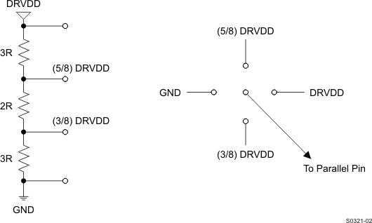 Figure 57. Simple Scheme to Configure Parallel Pins
7.5.2.3 Description of Parallel Pins
Table 4. SCLK Control Pin
| SCLK | DESCRIPTION |
|---|---|
| 0 | DEFAULT SPEED mode - Use for sampling frequencies > 25 MSPS, 3dB Gain. |
| DRVDD | LOW SPEED mode Enabled - Use for sampling frequencies ≤ 25 MSPS, 1dB Gain. |
Table 5. SDATA Control Pin
| SDATA | DESCRIPTION |
|---|---|
| 0 | Normal operation (Default) |
| DRVDD | STANDBY. This is a global power-down, where ADC, internal references and the output buffers are powered down. |
Table 6. SEN Control Pin
| SEN | DESCRIPTION |
|---|---|
| WITH CMOS INTERFACE | |
| 0 | CLKOUT Rising edge later by (3/36)Ts CLKOUT Falling edge later by (3/36)Ts |
| (3/8)DRVDD | CLKOUT Rising edge later by (5/36)Ts CLKOUT Falling edge later by (5/36)Ts |
| (5/8)DRVDD | CLKOUT Rising edge earlier by (3/36)Ts CLKOUT Falling edge earlier by (3/36)Ts |
| DRVDD | Default CLKOUT position |
| WITH LVDS INTERFACE | |
| 0 | CLKOUT Rising edge later by (7/36)Ts CLKOUT Falling edge later by (6/36)Ts |
| (3/8)DRVDD | CLKOUT Rising edge later by (7/36)Ts CLKOUT Falling edge later by (6/36)Ts |
| (5/8)DRVDD | CLKOUT Rising edge later by (3/36)Ts CLKOUT Falling edge later by (3/36)Ts |
| DRVDD | Default CLKOUT position |
Table 7. DFS Control Pin
| DFS | DESCRIPTION |
|---|---|
| 0 | 2s-complement data and DDR LVDS output (Default) |
| (3/8)DRVDD | 2s-complement data and parallel CMOS output |
| (5/8)DRVDD | Offset binary data and parallel CMOS output |
| DRVDD | Offset binary data and DDR LVDS output |
Table 8. MODE Control Pin
| MODE | DESCRIPTION |
|---|---|
| 0 | Internal reference |
| (3/8)AVDD | External reference |
| (5/8)AVDD | External reference |
| AVDD | Internal reference |
7.5.3 Serial Interface
The ADC has a set of internal registers, which can be accessed through the serial interface formed by the SEN (serial interface enable), SCLK (serial interface clock), SDATA (serial interface data), and RESET pins. After device power-up, the internal registers must be reset to the default values by applying a high-going pulse on RESET (of width greater than 10 ns), or by a high setting on the <RST> bit (D1 in register 0x6C).
A serial shift of bits into the device is enabled when the SEN pin is low. The serial data pin, SDATA, is latched at every falling edge of the SCLK pin when the SEN pin is active (low). The serial data is loaded into the register at every 16th SCLK falling edge when the SEN pin is low. If the word length exceeds a multiple of 16 bits, the excess bits are ignored. Data is loaded in multiples of 16-bit words within a single active SEN pulse.
The first 8 bits form the register address and the remaining 8 bits form the register data. The interface can work with a SCLK frequency from 20 MHz down to very low speeds (few Hertz) and also with non-50% SCLK duty cycle.
7.5.4 Register Initialization
After power-up, the internal registers must be reset to the default values which occurs in one of the following ways:
- A hardware reset by applying a high-going pulse on the RESET pin (of width greater than 10 ns) as shown in Figure 58.
- A software reset by using the serial interface and setting the <RST> bit (D1 in register 0x6C) to high. This configuration initializes the internal registers to the default values and then self-resets the <RST> bit to low. In this case the RESET pin is kept low.
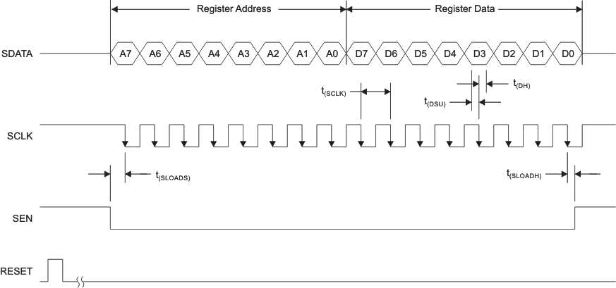 Figure 58. Serial Interface Timing Diagram
7.6 Register Maps
Table 9 gives a summary of all the modes that can be programmed through the serial interface.
Table 9. Summary of Functions Supported by Serial Interface(1) (2)
| REGISTER ADDRESS IN HEX |
REGISTER FUNCTIONS | |||||||
|---|---|---|---|---|---|---|---|---|
| A7 - A0 | D7 | D6 | D5 | D4 | D3 | D2 | D1 | D0 |
| 5D | <LF NOISE SUPPRESSION> | |||||||
| 62 | <CLKOUT POSN>
Output clock position programmability |
|||||||
| 63 | <STBY>
Global power down |
<DF>
DATA FORMAT - 2s complement or offset binary |
<LOW SPEED>
Enable low sampling frequency operation |
|||||
| 65 | <TEST PATTERN> – All 0s, all 1s, toggle, ramp, custom pattern | |||||||
| 68 | <GAIN>
Fine gain 0 dB to 6 dB, in 1-dB steps |
|||||||
| 69 | <CUSTOM A> Custom pattern (D7 TO D0) | |||||||
| 6A | <CUSTOM B> Custom pattern (D15 TO D8) | |||||||
| 6C | <ODI> Output data interface DDR LVDS or parallel CMOS |
|||||||
| 6D | <REF> Internal or external reference | |||||||
| 6E | <RST>
Software reset |
|||||||
| 7E | <DATA TERM>
Internal termination – data outputs |
<CLKOUT TERM>
Internal termination – output clock |
<LVDS CURR>
LVDS current programmability |
|||||
| 7F | <CURR DOUBLE>
LVDS current double |
|||||||
7.6.1 Register Description
This section explains each register function in detail.
Table 10. Register 5D
| A7 - A0 (hex) | D7 | D6 | D5 | D4 | D3 | D2 | D1 | D0 |
|---|---|---|---|---|---|---|---|---|
| 5D | <LF NOISE SUPPRESSION> |
| D0 | <LF NOISE SUPPRESSION> Low-Frequency Noise Suppression | |
| 0 | Disable low-frequency noise suppression | |
| 1 | Enable low-frequency noise suppression | |
Table 11. Register 62
| A7 - A0 (hex) | D7 | D6 | D5 | D4 | D3 | D2 | D1 | D0 |
|---|---|---|---|---|---|---|---|---|
| 62 | <CLKOUT POSN>
Output clock position programmability |
|||||||
| D4 - D0 | <CLKOUT POSN> Output Clock Position Programmability | |
| 00000 | Register value after reset (corresponds to default CLKOUT position) Setup/hold timings with this clock position are specified in the Timing Characteristics for LVDS and CMOS Modes table. |
|
| 00001 | Default CLKOUT position. Setup and hold timings with this clock position are specified in the Timing Characteristics for LVDS and CMOS Modes table. |
|
| XX011 | CMOS - Rising edge earlier by (3/36) Ts | |
| LVDS - Falling edge later by (3/36) Ts | ||
| XX101 | CMOS - Rising edge later by (3/36) Ts | |
| LVDS - Falling edge later by (6/36) Ts | ||
| XX111 | CMOS - Rising edge later by (5/36) Ts | |
| LVDS - Falling edge later by (6/36) Ts | ||
| 01XX1 | CMOS - Falling edge earlier by (3/36) Ts | |
| LVDS - Rising edge later by (3/36) Ts | ||
| 10XX1 | CMOS - Falling edge later by (3/36) Ts | |
| LVDS - Rising edge later by (7/36) Ts | ||
| 11XX1 | CMOS - Falling edge later by (5/36) Ts | |
| LVDS - Rising edge later by (7/36) Ts | ||
Table 12. Register 63
| A7 - A0 (hex) | D7 | D6 | D5 | D4 | D3 | D2 | D1 | D0 |
|---|---|---|---|---|---|---|---|---|
| 63 | <STBY>
Global power down |
<DF>
DATA FORMAT - 2s complement or offset binary |
<LOW SPEED>
Enable low sampling frequency operation |
| D3 | <DF> Output Data Format | |
| 0 | 2s-complement | |
| 1 | Offset binary | |
| D0 | <LOW SPEED> Low Sampling Frequency Operation | |
| 0 | DEFAULT SPEED mode (for Fs > 25 MSPS) | |
| 1 | LOW SPEED mode eabled (for Fs ≤ 25 MSPS) | |
| D7 | <STBY> Global STANDBY | |
| 0 | Normal operation | |
| 1 | Global power-down (includes ADC, internal references and output buffers) | |
Table 13. Register 65
| A7 - A0 (hex) | D7 | D6 | D5 | D4 | D3 | D2 | D1 | D0 |
|---|---|---|---|---|---|---|---|---|
| 65 | <TEST PATTERNS> — All 0s, all 1s, toggle, ramp, custom pattern | |||||||
| D7 - D5 | <TEST PATTERN> Outputs selected test pattern on data lines | |
| 000 | Normal operation | |
| 001 | All 0s | |
| 010 | All 1s | |
| 011 | Toggle pattern - alternate 1s and 0s on each data output and across data outputs | |
| 100 | Ramp pattern - Output data ramps from 0x0000 to 0xFFFF by one code every clock cycle | |
| 101 | Custom pattern - Outputs the custom pattern in CUSTOM PATTERN registers A and B | |
| 111 | Unused | |
Table 14. Register 68
| A7 - A0 (hex) | D7 | D6 | D5 | D4 | D3 | D2 | D1 | D0 |
|---|---|---|---|---|---|---|---|---|
| 68 | <GAIN> Fine gain 0 dB to 6 dB, in 1-dB steps | |||||||
| D3 - D0 | <GAIN> Programmable Fine Gain | |
| 0XXX | 1 dB | |
| 1000 | 0 dB | |
| 1001 | 1 dB, default register value after reset | |
| 1010 | 2 dB | |
| 1011 | 3 dB | |
| 1100 | 4 dB | |
| 1101 | 5 dB | |
| 1110 | 6 dB | |
Table 15. Register 69 and Register 6A
| A7 - A0 (hex) | D7 | D6 | D5 | D4 | D3 | D2 | D1 | D0 |
|---|---|---|---|---|---|---|---|---|
| 69 | <CUSTOM A> Custom pattern (D7–D0) | |||||||
| 6A | <CUSTOM B> Custom pattern (D15–D8) | |||||||
| Register 69 D7 - D0 |
<CUSTOM A> Custom pattern (D7–D0) | |
| Program bits D7 to D0 of custom pattern | ||
| Register 6A D15 - D8 |
<CUSTOM B> Custom pattern (D15–D8) | |
| Program bits D15 to D8 of custom pattern | ||
Table 16. Register 6C
| A7 - A0 (hex) | D7 | D6 | D5 | D4 | D3 | D2 | D1 | D0 |
|---|---|---|---|---|---|---|---|---|
| 6C | <ODI> Output data interface - DDR LVDS or parallel CMOS | |||||||
| D4 - D3 | <ODI> Output Interface | |
| 00 | default after reset, state of DFS pin determines interface type. See Table 7. | |
| 01 | DDR LVDS outputs, independent of state of DFS pin. | |
| 11 | Parallel CMOS outputs, independent of state of DFS pin. | |
Table 17. Register 6D
| A7 - A0 | D7 | D6 | D5 | D4 | D3 | D2 | D1 | D0 |
|---|---|---|---|---|---|---|---|---|
| 6D | <REF>
Internal or external reference |
| D4 | <REF> Reference | |
| 0 | Internal reference | |
| 1 | External reference mode, force voltage on VCM to set reference. | |
Table 18. Register 6E
| A7 - A0 | D7 | D6 | D5 | D4 | D3 | D2 | D1 | D0 |
|---|---|---|---|---|---|---|---|---|
| 6E | <RST> Software reset |
| D0 | <RST> Software resets the ADC | |
| 1 | Resets all registers to default values | |
Table 19. Register 7E
| A7 - A0 | D7 | D6 | D5 | D4 | D3 | D2 | D1 | D0 |
|---|---|---|---|---|---|---|---|---|
| 7E | <DATA TERM> Internal termination – data outputs | <CLKOUT TERM> Internal termination – output clock | <LVDS CURR> LVDS current programmability | |||||
| D1 - D0 | <LVDS CURR> LVDS Buffer Current Programmability | |
| 00 | 3.5 mA, default | |
| 01 | 2.5 mA | |
| 10 | 4.5 mA | |
| 11 | 1.75 mA | |
| D4 - D2 | <CLKOUT TERM> LVDS Buffer Internal Termination | |
| 000 | No internal termination | |
| 001 | 325 | |
| 010 | 200 | |
| 011 | 125 | |
| 100 | 170 | |
| 101 | 120 | |
| 110 | 100 | |
| 111 | 75 | |
| D7 - D5 | <DATA TERM> LVDS Buffer Internal Termination | |
| 000 | No internal termination | |
| 001 | 325 | |
| 010 | 200 | |
| 011 | 125 | |
| 100 | 170 | |
| 101 | 120 | |
| 110 | 100 | |
| 111 | 75 | |
Table 20. Register 7F
| A7 - A0 | D7 | D6 | D5 | D4 | D3 | D2 | D1 | D0 |
|---|---|---|---|---|---|---|---|---|
| 7F | <CURR DOUBLE> LVDS current double | |||||||
| D7 - D6 | <CURR DOUBLE> LVDS Buffer Internal Termination | |
| 00 | Value specified by <LVDS CURR> | |
| 01 | 2x data, 2x clockout currents | |
| 10 | 1x data, 2x clockout currents | |
| 11 | 2x data, 4x clockout currents | |
