JAJSE70 December 2016 ADS7046
PRODUCTION DATA.
- 1 特長
- 2 アプリケーション
- 3 概要
- 4 改訂履歴
- 5 Pin Configuration and Functions
- 6 Specifications
- 7 Parameter Measurement Information
- 8 Detailed Description
- 9 Application and Implementation
- 10Power Supply Recommendations
- 11Layout
- 12デバイスおよびドキュメントのサポート
- 13メカニカル、パッケージ、および注文情報
パッケージ・オプション
メカニカル・データ(パッケージ|ピン)
- RUG|8
サーマルパッド・メカニカル・データ
- RUG|8
発注情報
10 Power Supply Recommendations
10.1 AVDD and DVDD Supply Recommendations
The device has two separate power supplies: AVDD and DVDD.
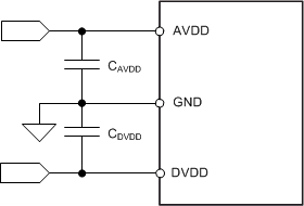
AVDD powers the analog blocks and is also used as the reference voltage for the analog-to-digital conversion. Use a low-noise, low-dropout regulator (LDO) or a discrete reference to supply AVDD (see the Reference and Application Information sections). Always set the AVDD supply to be greater than or equal to the maximum input signal to avoid code saturation. Decouple the AVDD pin to the GND pin with a 3.3-µF ceramic decoupling capacitor.
DVDD is used for the interface circuits. Decouple the DVDD pin to the GND pin with a 1-µF ceramic decoupling capacitor. Figure 49 shows the decoupling recommendations.
 Figure 49. Power-Supply Decoupling
10.2 Optimizing Power Consumed by the Device
In order to best optimize the power consumed by the device, use the following design considerations:
- Keep the analog supply voltage (AVDD) in the specified operating range and equal to the maximum analog input voltage.
- Keep the digital supply voltage (DVDD) in the specified operating range and at the lowest value supported by the host controller.
- Reduce the load capacitance on the SDO output.
- Run the device at the optimum throughput. Power consumption reduces proportionally with the throughput.
10.2.1 Estimating Digital Power Consumption
The current consumption from the DVDD supply depends on the DVDD voltage, the load capacitance on the SDO pin (CLOAD-SDO), and the output code, and can be calculated as:
where
- CLOAD-SDO = Load capacitance on the SDO pin
- V = DVDD supply voltage
- f = Frequency of transitions on the SDO output
The number of transitions on the SDO output depends on the output code, and thus changes with the analog input. The maximum value of f occurs when data output on the SDO change on every SCLK (that is, for output codes of AAAh or 555h). With an output code of AAAh or 555h, f = 18 MHz and when CLOAD-SDO = 20 pF and DVDD = 1.8 V, IDVDD = 650 µA.