JAJSE74 December   2017 ADS7054

PRODUCTION DATA.  

  1. 特長
  2. アプリケーション
  3. 概要
  4. 改訂履歴
  5. Pin Configuration and Functions
  6. Specifications
    1. 6.1 Absolute Maximum Ratings
    2. 6.2 ESD Ratings
    3. 6.3 Recommended Operating Conditions
    4. 6.4 Thermal Information
    5. 6.5 Electrical Characteristics
    6. 6.6 Timing Requirements
    7. 6.7 Switching Characteristics
    8. 6.8 Typical Characteristics
  7. Parameter Measurement Information
    1. 7.1 Digital Voltage Levels
  8. Detailed Description
    1. 8.1 Overview
    2. 8.2 Functional Block Diagram
    3. 8.3 Feature Description
      1. 8.3.1 Product Family
      2. 8.3.2 Analog Input
      3. 8.3.3 Reference
      4. 8.3.4 ADC Transfer Function
    4. 8.4 Device Functional Modes
      1. 8.4.1 ACQ State
      2. 8.4.2 CNV State
      3. 8.4.3 OFFCAL State
        1. 8.4.3.1 Offset Calibration on Power-Up
        2. 8.4.3.2 Offset Calibration During Normal Operation
  9. Application and Implementation
    1. 9.1 Application Information
    2. 9.2 Typical Applications
      1. 9.2.1 2-Channel, Simultaneous Sampling Data Acquisition Using the ADS7054
        1. 9.2.1.1 Design Requirements
        2. 9.2.1.2 Detailed Design Procedure
          1. 9.2.1.2.1 Low Distortion Charge Kickback Filter Design
          2. 9.2.1.2.2 Input Amplifier Selection
          3. 9.2.1.2.3 Reference Circuit
        3. 9.2.1.3 Application Curves
      2. 9.2.2 Improving Precision of Single-Ended Signal Source Measurements Using the ADS7054
        1. 9.2.2.1 Design Requirements
        2. 9.2.2.2 Detailed Design Procedure
        3. 9.2.2.3 Application Curve
  10. 10Power Supply Recommendations
    1. 10.1 AVDD and DVDD Supply Recommendations
    2. 10.2 Optimizing Power Consumed by the Device
      1. 10.2.1 Estimating Digital Power Consumption
  11. 11Layout
    1. 11.1 Layout Guidelines
    2. 11.2 Layout Example
  12. 12デバイスおよびドキュメントのサポート
    1. 12.1 デバイス・サポート
      1. 12.1.1 開発サポート
    2. 12.2 ドキュメントのサポート
      1. 12.2.1 関連資料
    3. 12.3 ドキュメントの更新通知を受け取る方法
    4. 12.4 コミュニティ・リソース
    5. 12.5 商標
    6. 12.6 静電気放電に関する注意事項
    7. 12.7 Glossary
  13. 13メカニカル、パッケージ、および注文情報

パッケージ・オプション

メカニカル・データ(パッケージ|ピン)
サーマルパッド・メカニカル・データ
発注情報

Layout

Layout Guidelines

Figure 47 shows a typical connection diagram for the ADS7054.

ADS7054 layout_sch_diff_sbas769.gif Figure 47. Typical Connection Diagram

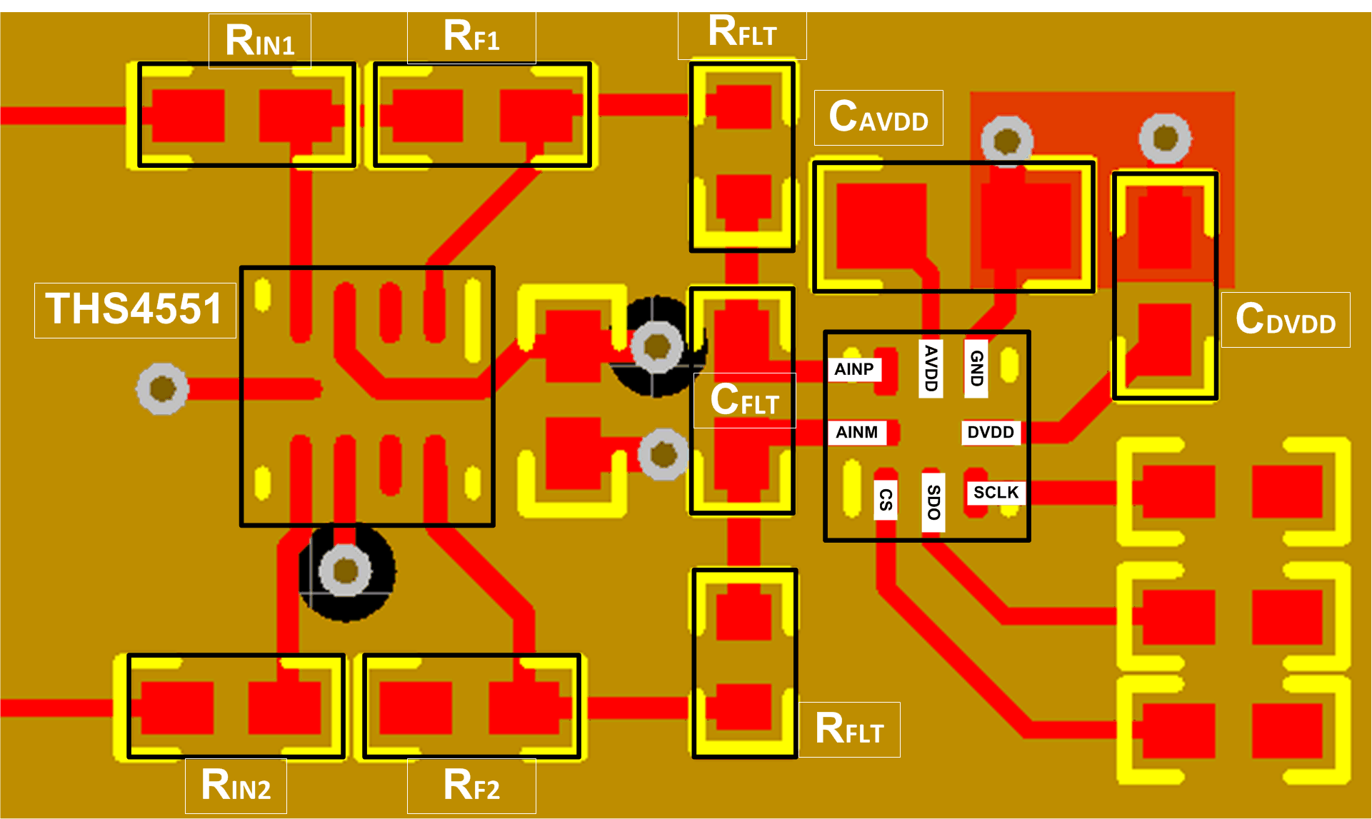
Figure 48 depicts a board layout example for the device for the typical connection diagram in Figure 47. The key considerations for layout are:

  • Use a solid ground plane underneath the device and partition the PCB into analog and digital sections
  • Avoid crossing digital lines with the analog signal path and keep the analog input signals and the reference input signals away from noise sources.
  • The power sources to the device must be clean and well-bypassed. Use CAVDD decoupling capacitors in close proximity to the analog (AVDD) power-supply pin.
  • Use a CDVDD decoupling capacitor close to the digital (DVDD) power-supply pin.
  • Avoid placing vias between the AVDD and DVDD pins and the bypass capacitors.
  • Connect the ground pin to the ground plane using a short, low-impedance path.
  • Place the charge kickback filter components close to the device.

Among ceramic surface-mount capacitors, COG (NPO) ceramic capacitors are recommended because these components provide the most stable electrical properties over voltage, frequency, and temperature changes.

Layout Example

ADS7054 layout_layout_diff_sbas769.gif Figure 48. Example Layout