JAJSJL9B March   2021  – September 2024 ADS7067

PRODUCTION DATA  

  1.   1
  2. 特長
  3. アプリケーション
  4. 概要
  5. Pin Configuration and Functions
  6. Specifications
    1. 5.1 Absolute Maximum Ratings
    2. 5.2 ESD Ratings
    3. 5.3 Recommended Operating Conditions
    4. 5.4 Thermal Information
    5. 5.5 Electrical Characteristics
    6. 5.6 Timing Requirements
    7. 5.7 Switching Characteristics
    8. 5.8 Timing Diagrams
    9. 5.9 Typical Characteristics
  7. Detailed Description
    1. 6.1 Overview
    2. 6.2 Functional Block Diagram
    3. 6.3 Feature Description
      1. 6.3.1  Analog Input and Multiplexer
      2. 6.3.2  Reference
        1. 6.3.2.1 External Reference
        2. 6.3.2.2 Internal Reference
      3. 6.3.3  ADC Transfer Function
      4. 6.3.4  ADC Offset Calibration
      5. 6.3.5  Programmable Averaging Filters
      6. 6.3.6  CRC on Data Interface
      7. 6.3.7  Oscillator and Timing Control
      8. 6.3.8  Diagnostic Modes
        1. 6.3.8.1 Bit-Walk Test Mode
        2. 6.3.8.2 Fixed Voltage Test Mode
      9. 6.3.9  Output Data Format
        1. 6.3.9.1 Status Flags
        2. 6.3.9.2 Output CRC (Device to Host)
        3. 6.3.9.3 Input CRC (Host to Device)
      10. 6.3.10 Device Programming
        1. 6.3.10.1 Enhanced-SPI Interface
        2. 6.3.10.2 Daisy-Chain Mode
        3. 6.3.10.3 Register Read/Write Operation
          1. 6.3.10.3.1 Register Write
          2. 6.3.10.3.2 Register Read
            1. 6.3.10.3.2.1 Register Read With CRC
    4. 6.4 Device Functional Modes
      1. 6.4.1 Device Power-Up and Reset
      2. 6.4.2 Manual Mode
      3. 6.4.3 On-the-Fly Mode
      4. 6.4.4 Auto-Sequence Mode
    5. 6.5 ADS7067 Registers
  8. Application and Implementation
    1. 7.1 Application Information
    2. 7.2 Typical Application
      1. 7.2.1 Design Requirements
      2. 7.2.2 Detailed Design Procedure
        1. 7.2.2.1 Charge-Kickback Filter and ADC Amplifier
      3. 7.2.3 Application Curve
    3. 7.3 Power Supply Recommendations
      1. 7.3.1 AVDD and DVDD Supply Recommendations
    4. 7.4 Layout
      1. 7.4.1 Layout Guidelines
      2. 7.4.2 Layout Example
  9. Device and Documentation Support
    1. 8.1 Device Support
      1. 8.1.1 Development Support
    2. 8.2 Documentation Support
      1. 8.2.1 Related Documentation
    3. 8.3 ドキュメントの更新通知を受け取る方法
    4. 8.4 サポート・リソース
    5. 8.5 Trademarks
    6. 8.6 静電気放電に関する注意事項
    7. 8.7 用語集
  10. Revision History
  11. 10Mechanical, Packaging, and Orderable Information

パッケージ・オプション

メカニカル・データ(パッケージ|ピン)
サーマルパッド・メカニカル・データ
発注情報

AVDD and DVDD Supply Recommendations

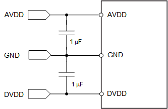
The ADS7067 has two separate power supplies: AVDD and DVDD. The device operates on AVDD; DVDD is used for the interface circuits. AVDD and DVDD can be independently set to any value within the permissible ranges. As shown in Figure 7-3, decouple the AVDD and DVDD pins individually with 1-µF ceramic decoupling capacitors.
ADS7067 Power-Supply DecouplingFigure 7-3 Power-Supply Decoupling