JAJSGH2B November 2017 – September 2022 ADS7142-Q1
PRODUCTION DATA
- 1 特長
- 2 アプリケーション
- 3 概要
- 4 Revision History
- 5 Pin Configuration and Functions
-
6 Specifications
- 6.1 Absolute Maximum Ratings
- 6.2 ESD Ratings
- 6.3 Recommended Operating Conditions
- 6.4 Thermal Information
- 6.5 Electrical Characteristics: All Modes
- 6.6 Electrical Characteristics: Manual Mode
- 6.7 Electrical Characteristics: Autonomous Modes
- 6.8 Electrical Characteristics: High Precision Mode
- 6.9 Timing Requirements
- 6.10 Switching Characteristics
- 6.11 Timing Diagrams
- 6.12 Typical Characteristics: All Modes
- 6.13 Typical Characteristics: Manual Mode
- 6.14 Typical Characteristics: Autonomous Modes
- 6.15 Typical Characteristics: High-Precision Mode
-
7 Detailed Description
- 7.1 Overview
- 7.2 Functional Block Diagram
- 7.3 Feature Description
- 7.4 Device Functional Modes
- 7.5 Programming
- 7.6 Register Map
- 8 Application and Implementation
- 9 Device and Documentation Support
- 10Mechanical, Packaging, and Orderable Information
パッケージ・オプション
メカニカル・データ(パッケージ|ピン)
- DQC|10
サーマルパッド・メカニカル・データ
- DQC|10
発注情報
7.3.9 Digital Window Comparator
The internal digital window comparator is available in all modes. In autonomous modes with thresholds monitoring and diagnostics, the digital window comparator controls the filling of the data into the FIFO and the output of the ALERT pin. In the remaining modes, the digital window comparator only controls the output of the ALERT pin. Figure 7-9 provides the block diagram for digital window comparator.
 Figure 7-9 Digital Comparator Block Diagram
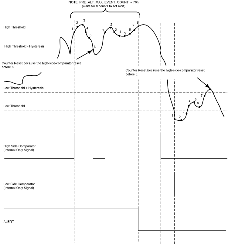
The low-side threshold, high-side threshold, and hysteresis parameters are independently programmable for each input channel. Figure 7-10 illustrates the comparison thresholds and hysteresis for the two comparators. A pre-ALERT event counter after each comparator counts the output of the comparator and sets the latched flags. The pre-ALERT event counter settings are common to the two channels.
 Figure 7-10 Thresholds, Hysteresis,
and Event Counter for the Digital Window Comparator
Figure 7-10 Thresholds, Hysteresis,
and Event Counter for the Digital Window ComparatorThe DWC_BLOCK_EN bit in the ALERT_DWC_EN register enables and disables the complete digital window comparator block (disabled at power-up) and the ALERT_EN_CHx bits in the ALERT_CHEN register enables the digital window comparator for individual channels. Possible responses when using the digital comparator when a new ADC conversion is completed include:
- The output of the high-side comparator transitions to a logic high when the conversion result is greater than the high threshold. This comparator resets when the conversion result is less than the high threshold – hysteresis.
- The output of the low-side comparator transitions to a logic high when the conversion result is less than the low threshold. This comparator resets when the conversion result is greater than the low threshold + hysteresis.
- When the output of either the high-side or low-side comparator transitions high, the pre-ALERT event counter begins to increment for each subsequent conversion. This counter continues to increment until the value stored in the PRE_ALT_MAX_EVENT_COUNT register is reached. When the counter reaches PRE_ALT_MAX_EVENT_COUNT, the alert becomes active and sets the latched flags. If the comparator output becomes zero before the counter reaches PRE_ALT_MAX_EVENT_COUNT, then the event counter is reset to zero, ALERT is not set, and the latched flag is not set.
Therefore, the latched flags (high and low) for the channel are updated only if the respective comparator output remains 1 for the specified number of consecutive conversions (set by PRE_ALT_MAX_EVENT_COUNT).
The latched flags can be read from the ALERT_LOW_FLAGS and ALERT_HIGH_FLAGS registers. To clear a latched flag, write 1 to the applicable bit location. The ALERT pin status is re-evaluated when an applicable latched flag is set or is cleared.
The response time for the ALERT pin can be estimated by Equation 6
where:
- k = Number of channels enabled in device sequence
- nCLK = Number of clocks used by device for one conversion cycle
- Oscillator timer period = tLPO or tHSO depending on the OSC_SEL value; see the Section 6 section for tLPO or tHSO