JAJSHX7A September 2010 – September 2019 ADS7947 , ADS7948 , ADS7949
PRODUCTION DATA.
- 1 特長
- 2 アプリケーション
- 3 概要
- 4 改訂履歴
- 5 Device Comparison Table
- 6 Pin Configuration and Functions
-
7 Specifications
- 7.1 Absolute Maximum Ratings
- 7.2 ESD Ratings
- 7.3 Recommended Operating Conditions: ADS794x (12-, 10-, 8-Bit)
- 7.4 Thermal Information
- 7.5 Electrical Characteristics: ADS7947 (12-Bit)
- 7.6 Electrical Characteristics: ADS7948 (10-Bit)
- 7.7 Electrical Characteristics: ADS7949 (8-Bit)
- 7.8 Timing Requirements
- 7.9 Switching Characteristics
- 7.10 Typical Characteristics: ADS7947, ADS7948, ADS7949
- 7.11 Typical Characteristics: ADS7947 (12-Bit)
- 8 Detailed Description
- 9 Application and Implementation
- 10Power Supply Recommendations
- 11Layout
- 12デバイスおよびドキュメントのサポート
- 13メカニカル、パッケージ、および注文情報
パッケージ・オプション
メカニカル・データ(パッケージ|ピン)
- RTE|16
サーマルパッド・メカニカル・データ
- RTE|16
発注情報
8.3.1 Multiplexer and ADC Input
The devices feature pseudo-differential inputs with a double-pole, double-throw multiplexer. The negative inputs (AINxN) can accept swings of ±0.2 V; the positive inputs (AINxP) allow signals in the range of 0 V to VREF over the negative input. The ADC converts the difference in voltage: VAINxP – VAINxN. This feature can be used in multiple ways.
Two signals can be connected from different sensors with unequal ground potentials (within ±0.2 V) to a single ADC. The pseudo-differential ADC rejects common-mode offset and noise. This feature also allows the use of a single-supply op amp. The signal and the AINxN input can be offset by +0.2 V, which provides the ground clearance needed for a single-supply op amp.
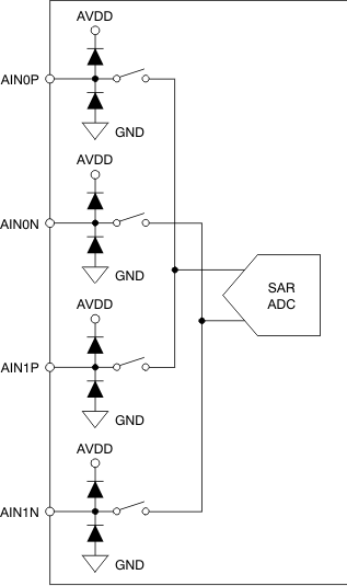
Figure 39 shows the electrostatic discharge (ESD) diodes to supply and ground at every analog input. Make sure that these diodes do not turn on by keeping the supply voltage within the specified input range.
 Figure 39. Analog Inputs
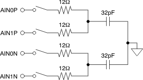
 Figure 40 shows an equivalent circuit of the multiplexer and ADC sampling stage. The positive and negative inputs are separately sampled on 32-pF sampling capacitors. The multiplexer and sampling switches are represented by an ideal switch in series with a 12-Ω resistance. During sampling, the devices connect the 32-pF sampling capacitor to the ADC driver. This connection creates a glitch at the device input. TI recommends connecting a capacitor across the AINxP and AINxN terminals to reduce this glitch. A driving circuit must have sufficient bandwidth to settle this glitch within the acquisition time.
 Figure 40. Input Sampling Stage Equivalent Circuit
(See the Application Information section for details on the driving circuit.)
Figure 41 shows a timing diagram for the ADC analog input channel selection. As shown in Figure 41, the CH SEL signal selects the analog input channel to the ADC. CH SEL = 0 selects channel 0 (AIN0P – AIN0N) and CH SEL = 1 selects channel 1 (AIN1P – AIN1N). It is recommended not to toggle the CH SEL signal during an ADC acquisition phase until the device detects the first valid SCLK rising edge after the device samples the analog input. If CH SEL is toggled during this period, an erroneous output code can result because the device might detect an unsettled analog input.
CH SEL can be toggled at any time during the window specified in Figure 41; however, TI recommends selecting the desired channel after the first SCLK rising edge and before the second SCLK rising edge. This timing ensures that the multiplexer output is settled before the ADC starts acquisition of the analog input.

NOINDENT:
N indicates the 14th SCLK rising edge for the ADS7947 (12 bit), the 11th rising edge for the ADS7948 (10 bit), and the ninth rising edge for the ADS7949 (8 bit).